Pixel defining structure, display substrate and manufacturing method thereof, and display device

A technology for pixel definition and display substrate, applied in semiconductor/solid-state device manufacturing, electrical components, electrical solid-state devices, etc. The effect of climbing too high

Active Publication Date: 2018-03-20
BOE TECH GRP CO LTD
View PDF3 Cites 18 Cited by
  • Summary
  • Abstract
  • Description
  • Claims
  • Application Information

AI Technical Summary

Problems solved by technology

However, if the material of the pixel defining layer is reduced to 1um, the amount of ink droplets that can be contained in the sub-pixel area will be reduced. Therefore, reducing the material thickness of the pixel defining layer to suppress the climbing of ink droplets and maintain the loading capacity of ink droplets cannot be achieved at the same time. Satisfy

Method used


Image

  • Pixel defining structure, display substrate and manufacturing method thereof, and display device
  • Pixel defining structure, display substrate and manufacturing method thereof, and display device
  • Pixel defining structure, display substrate and manufacturing method thereof, and display device

Examples


Embodiment Construction

[0034] In order to enable those skilled in the art to better understand the technical solution of the present invention, the technical solution in the present invention will be clearly and completely described below in conjunction with the accompanying drawings. Obviously, the described embodiments are part of the embodiments of the present invention, and Not all examples. Based on the embodiments of the present invention, all other embodiments obtained by persons of ordinary skill in the art without making creative efforts belong to the protection scope of the present invention.

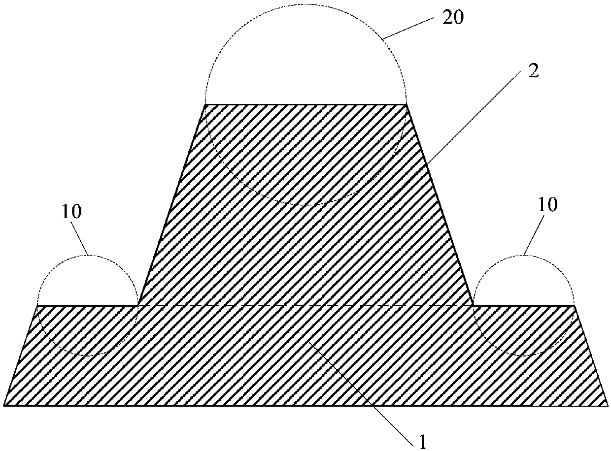
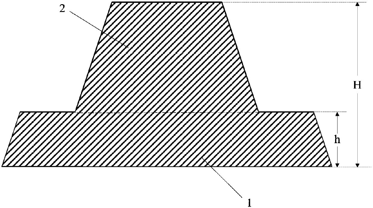
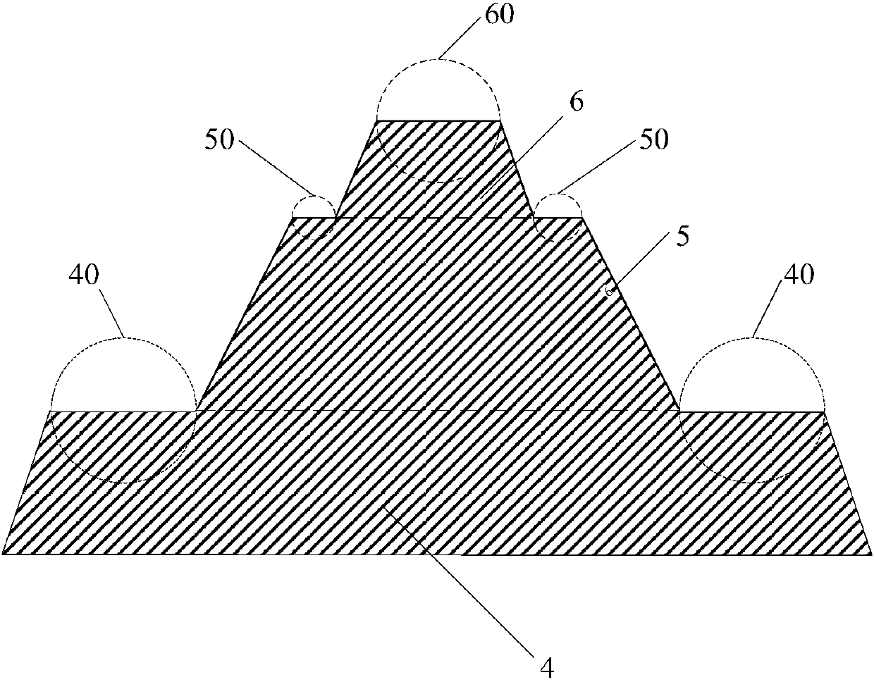
[0035] figure 1 A schematic structural diagram of a pixel defining structure provided in Embodiment 1 of the present invention, as shown in figure 1 As shown, the pixel defining structure includes at least two layers of ladder structures arranged in a ladder shape.

[0036] In this embodiment, preferably, the pixel defining structure includes a two-layer ladder structure arranged in a ladder shape...


PUM


Abstract

The invention discloses a pixel defining structure, a display substrate and a manufacturing method thereof, and a display device. The pixel defining structure includes at least two layers of step structures arranged in a ladder shape. When limiting ink droplets from flowing into a sub pixel area, the pixel defining structure can prevent the ink droplets from climbing too high on one hand and can maintain the loading capacity of the ink droplets on the other hand.

Description

technical field [0001] The invention relates to the field of display devices, in particular to a pixel defining structure, a display substrate, a manufacturing method thereof, and a display device. Background technique [0002] Compared with Liquid Crystal Display (LCD), Organic Light-Emitting Diode (OLED) has the advantages of self-illumination, fast response, wide viewing angle, high brightness, bright color, light and thin, etc. next generation display technology. [0003] OLED film-forming methods mainly include evaporation process or solution process. The evaporation process is relatively mature in small-scale applications, and this technology has been applied in mass production. The solution process OLED film-forming methods mainly include inkjet printing, nozzle coating, spin coating, screen printing, etc. Among them, inkjet printing technology is considered to be a large-scale OLED technology due to its high material utilization rate and large-scale realization. A...

Claims


Application Information

Patent Timeline
Patent Type & Authority Applications(China)
IPC IPC(8): H01L27/32H01L51/56
CPCH10K59/122H10K59/121H10K71/00
Inventor 王辉锋甘静
Owner BOE TECH GRP CO LTD
Why Eureka
Try Eureka