Flexible display device and manufacturing method thereof
A flexible display device and flexible display technology, applied in semiconductor devices, electrical components, circuits, etc., can solve problems such as short circuit of metal wires
- Summary
- Abstract
- Description
- Claims
- Application Information
AI Technical Summary
Problems solved by technology
Method used
Image
Examples
Embodiment Construction
[0036] As mentioned in the background section, in the prior art, photoresist remains between the metal traces due to the slope angle of the bending area, which leads to a short circuit between the metal traces.
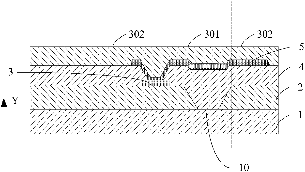
[0037] Based on this, the present invention provides a flexible display panel, such as image 3 As shown, according to the state of use of the flexible display panel, it can be divided into a bending area 301 and a non-bending area 302 . From the vertical hierarchical structure of the flexible display panel, it may include: a flexible substrate 1 , an inorganic layer 2 , a first metal wiring 3 , a planarization layer 4 and a second metal wiring 5 .
[0038] Specifically, please combine Figure 4 , Figure 4 A schematic diagram of the specific structure of each layer in a flexible display panel provided in this embodiment, wherein the inorganic layer 2 may include a buffer layer 401, a gate insulating layer 402, a first insulating layer 403, and a source-drain insula...
PUM
| Property | Measurement | Unit |
|---|---|---|
| Thickness | aaaaa | aaaaa |
| Thickness | aaaaa | aaaaa |
Abstract
Description
Claims
Application Information


