
Insulated gate bipolar transistor advanced active embedded circuit

A technology of bipolar transistors and insulated gates, applied in the direction of transistors, circuits, electrical components, etc., can solve the problem of no practical application value, failure to achieve clamping effect, active clamping technology can not achieve active clamping effect, etc. question

Inactive Publication Date: 2018-03-27
北京合瑞华思科技有限公司
View PDF2 Cites 10 Cited by
  • Summary
  • Abstract
  • Description
  • Claims
  • Application Information

AI Technical Summary

Problems solved by technology

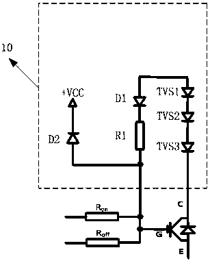
The disadvantage is: since the gate of the IGBT is in a low-resistance state when it is turned off, the breakdown current of the TVS diode is shunted by the circuit in the low-resistance state, so that the gate voltage of the IGBT is almost impossible to be pulled up, and the ideal embedding cannot be achieved. bit effect, so the present invention calls the method a basic active clamping circuit
But this patented technology has no practical application value, because first of all, this patented technology adds the function of active clamping voltage threshold adjustment on the basis of the existing method 2. As described in method 2, the active clamping technology of method 2 reaches Less than the ideal active clamping effect; secondly, during the dynamic turn-on process of the IGBT, the voltage between the collector and the emitter will not exceed the DC bus voltage, and will not be affected by the fluctuation of the DC bus voltage. Moreover, at this time The gate voltage of the IGBT is already at a high level of about 15V. Even if the active clamping circuit reduces the operating voltage threshold of the active clamping circuit through the bypass part of the transient suppression diode mentioned in the patent, the active clamping circuit The circuit works, and it will not pull the gate voltage of the IGBT to a voltage higher than 15V. Therefore, when the IGBT is turned on in the above patent, the voltage threshold of the active clamping circuit or the operating voltage point is reduced by bypassing part of the transient suppression diode. any meaning

Method used


Image

  • Insulated gate bipolar transistor advanced active embedded circuit
  • Insulated gate bipolar transistor advanced active embedded circuit
  • Insulated gate bipolar transistor advanced active embedded circuit

Examples


Embodiment Construction

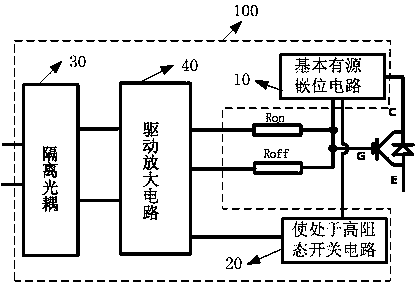
[0027] An embodiment of the present invention provides an IGBT advanced active clamping circuit.

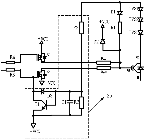
[0028] In order to make the object, technical solution and advantages of the present invention clearer, the present invention will be described in detail below in conjunction with the accompanying drawings and specific embodiments. Apparently, the described embodiment is only one embodiment of the present invention, not all. What the patent of the present invention needs to protect is the design method of the advanced active clamping circuit, that is: when the active clamping circuit operates, the gate of the IGBT It is in a high-impedance state with the negative power supply -VCC of the drive power supply. For those skilled in the art, all other embodiments obtained without any creative work belong to the protection scope of the present invention.

[0029] The following will be described in detail through examples.

[0030] The terms "first", "second", "third", etc. (if any) i...


PUM


Abstract

The invention discloses an insulated gate bipolar transistor advanced active embedded circuit comprising a basic active embedded circuit, a switch circuit which enables the output of a drive amplification circuit to be in a high-impedance state, an isolation optical coupling circuit and the drive amplifying circuit. The basic active embedded circuit is used for suppressing transient overvoltage occurring between a collector and a transmitter of the insulated gate bipolar transistor; the switch circuit which enables the output of the drive amplification circuit to be in the high-impedance stateis used for enabling the output of the drive amplification circuit to be in the high-impedance state; the isolation optical coupling circuit is used for preliminarily amplifying a drive signal and achieving electric isolation of strong and weak electricity; and the drive amplifying circuit is used for amplifying the drive signal output by the optical coupling circuit. According to the technical scheme provided by the embodiment of the invention, the reliable work of the insulated gate bipolar transistor can be more effectively and safely ensured.

Description

technical field [0001] The present invention relates to the field of circuit technology, in particular to an advanced active clamping circuit of an insulated gate bipolar transistor (Insulated Gate Bipolar Transistor, hereinafter referred to as "IGBT"). Background technique [0002] As an important power switching device, IGBT has been widely used in many fields of the national economy, such as: power transmission and distribution, motor drive, new energy vehicles, photovoltaic and wind power and other new energy inverters. When the IGBT is turned off, the rate of change of the collector current is high. Due to the stray inductance of the main circuit, a high surge peak voltage is generated between the collector and the emitter of the IGBT. The surge peak voltage is likely to exceed The safe working area of ​​the IGBT, thus damaging the IGBT. The basic principle of the active clamping is that when the undesired surge peak voltage appears, the active clamping circuit quickly...

Claims


Application Information

Patent Timeline
IPC IPC(8): H02M1/32H03K17/082
CPCH02M1/32H03K17/0826
Inventor 单升华
Owner 北京合瑞华思科技有限公司
Learn More