Double-layer ITO conductive film used for touch screen and manufacturing method

A conductive film, touch screen technology, applied in cable/conductor manufacturing, conductive layers on insulating carriers, circuits, etc., can solve the problems of short service life, high resistivity, poor light transmittance, etc. The effect of reducing resistivity and increasing service life

Inactive Publication Date: 2018-03-30
JIANGSU RIJIU OPTOELECTRONICS LTD
View PDF3 Cites 0 Cited by
  • Summary
  • Abstract
  • Description
  • Claims
  • Application Information

AI Technical Summary

Problems solved by technology

Due to the influence of its thickness on the crystallization process, the existing ITO conductive film has problems such as high resistivity, poor light transmittance and short service life.

Method used


Image

  • Double-layer ITO conductive film used for touch screen and manufacturing method
  • Double-layer ITO conductive film used for touch screen and manufacturing method

Examples


Embodiment

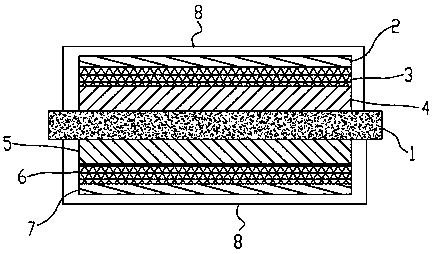
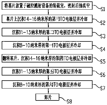
[0041] refer to figure 1 , a double-layer ITO conductive film for a touch screen, comprising a substrate 1 and an upper ITO electrode layer and a lower ITO electrode layer respectively deposited on both sides of the substrate 1; The first ITO electrode layer 2, the second ITO electrode layer 3 and the third ITO electrode layer 4, the third ITO electrode layer 4 is deposited on the substrate 1; the lower ITO electrode layer includes sequential stacking and thickness The fourth ITO electrode layer 5 , the fifth ITO electrode layer 6 and the sixth ITO electrode layer 7 are successively reduced, and the fourth ITO electrode layer 5 is deposited on the substrate 1 .

[0042] In another embodiment, the substrate 1 has a thickness of 150 microns, or 175 microns or 200 microns, and the substrate 1 is made of polyethylene terephthalate resin.

[0043] In another embodiment, an insulating electrode protection layer 8 is provided outside the first ITO electrode layer 2 and the sixth ITO...


PUM

PropertyMeasurementUnit
thicknessaaaaaaaaaa
thicknessaaaaaaaaaa
thicknessaaaaaaaaaa

Abstract

The invention discloses a double-layer ITO conductive film used for a touch screen. The conductive film comprises a substrate, an upper ITO electrode layer and a lower ITO electrode layer, wherein theupper ITO electrode layer and the lower ITO electrode layer are deposited on two sides of the substrate respectively. The upper ITO electrode layer comprises a first ITO electrode layer, a second ITOelectrode layer and a third ITO electrode layer which are successively stacked and arranged, and thicknesses of the first ITO electrode layer, the second ITO electrode layer and the third ITO electrode layer are successively increased. The third ITO electrode layer is deposited on the substrate. The lower ITO electrode layer comprises a fourth ITO electrode layer, a fifth ITO electrode layer anda sixth ITO electrode layer which are successively stacked and arranged, and the thicknesses of the fourth ITO electrode layer, the fifth ITO electrode layer and the sixth ITO electrode layer are successively decreased. The fourth ITO electrode layer is deposited on the substrate. The invention also provides a manufacturing method of the double-layer ITO conductive film used for the touch screen.The conductive film possesses advantages of low resistivity, high light transmittance, a long service life and the like.

Description

technical field [0001] The invention belongs to the technical field of touch screen conductive films, in particular to a double-layer ITO conductive film for a touch screen and a preparation method thereof. Background technique [0002] The touch screen has been widely used in mobile phones, tablet computers and other display screens. As an input device that significantly improves the human-machine interface, it has the advantages of intuitive simplicity, fast response, space saving and easy operation and communication. ITO conductive film is commonly used in the preparation of touch screens. ITO conductive film refers to a transparent conductive film obtained by sputtering a transparent ITO conductive film coating on a transparent organic film material by magnetron sputtering. ITO (Indium Tin Oxides, Indium Tin Metal Oxide), as an N-type oxide semiconductor used, is widely used in the touch screen field. Due to the influence of its thickness on the crystallization process,...

Claims


Application Information

Patent Timeline
Patent Type & Authority Applications(China)
IPC IPC(8): H01B5/14H01B13/00G06F3/044
CPCH01B5/14G06F3/044G06F2203/04103H01B13/00
Inventor 温泉
Owner JIANGSU RIJIU OPTOELECTRONICS LTD
Why Eureka
Try Eureka