Micro LED transfer apparatus and transfer method and manufacturing method of transfer apparatus

A technology of a transport device and a manufacturing method, which is applied in the manufacture of semiconductor/solid-state devices, electrical components, circuits, etc., can solve the problems of increasing the manufacturing cost and process complexity of the transport device.

Active Publication Date: 2018-03-30
SHANGHAI TIANMA MICRO ELECTRONICS CO LTD
View PDF4 Cites 46 Cited by
  • Summary
  • Abstract
  • Description
  • Claims
  • Application Information

AI Technical Summary

Problems solved by technology

However, making multiple CMOS switch circuits on the transfer device i...

Method used


Image

  • Micro LED transfer apparatus and transfer method and manufacturing method of transfer apparatus
  • Micro LED transfer apparatus and transfer method and manufacturing method of transfer apparatus
  • Micro LED transfer apparatus and transfer method and manufacturing method of transfer apparatus

Examples


Embodiment Construction

[0081] As mentioned in the background technology, the existing Micro LED transfer device controls the working state of the transfer unit through the micro switch connected to the transfer unit. Since each micro switch is a CMOS switch circuit, and the manufacturing process of the CMOS switch circuit Complicated, thus resulting in high manufacturing cost of the transfer device.

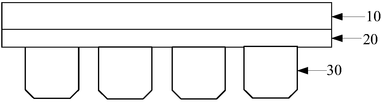
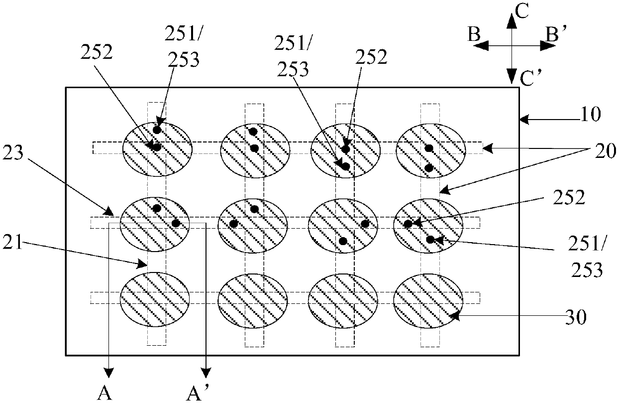
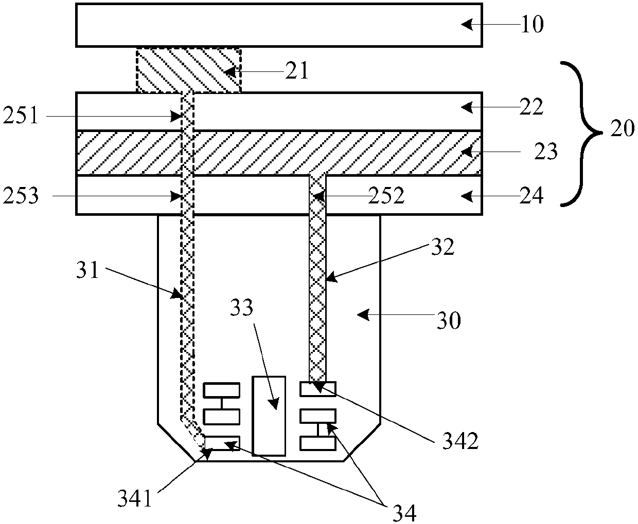
[0082] Based on this, the present invention provides a Micro LED transfer device, which reduces the manufacturing cost of the Micro LED transfer device compared with the prior art, such as figure 1 As shown, it is a cross-sectional view of the Micro LED transfer device. The transfer device includes: a transfer substrate 10, a drive electrode 20 located on the transfer substrate 10, and a drive electrode 20 located on the side away from the transfer substrate 10. A translocation unit array, the translocation unit array comprises a plurality of translocation units 30 .

[0083] Wherein, the driving elec...


PUM


Abstract

The invention provides a Micro LED transfer apparatus. The Micro LED transfer apparatus comprises a transfer substrate, a driving electrode and a transfer unit array; the transfer unit array comprisesa plurality of transfer units; the driving electrode is a conductive transmission line; one end of the driving electrode is directly connected with a driving chip while the other end is electricallyconnected with the transfer units; and a driving voltage output by the driving chip is transmitted by the driving electrode to be directly applied to the transfer units so as to enable the transfer units to generate electromagnetic force, or thermal energy or electrostatic in order to adsorb the Micro LED. The manufacturing cost of the Micro LED transfer apparatus is lowered on the basis of not influencing the Micro LED transfer effect.

Description

technical field [0001] The present invention relates to the field of display technology, and more specifically, to a Micro LED transfer device, a transfer method and a manufacturing method thereof. Background technique [0002] Light Emitting Diode (LED) is an optoelectronic semiconductor element that can convert current into a specific wavelength range. Its light-emitting principle is the energy difference between electrons moving between n-type semiconductors and p-type semiconductors, releasing energy in the form of light , so light-emitting diodes are called cold light sources, which have the advantages of low power consumption, small size, high brightness, easy matching with integrated circuits, and high reliability, and are widely used as light sources. Moreover, with the maturity of LED technology, the technology of directly using LEDs as self-luminous display dot pixels of LED displays or Micro LED (ie, micro LED) displays is gradually being widely used. [0003] Am...

Claims


Application Information

Patent Timeline
IPC IPC(8): H01L21/683H01L21/673
CPCH01L21/673H01L21/68714H01L21/68778
Inventor 李飞
Owner SHANGHAI TIANMA MICRO ELECTRONICS CO LTD
Why Eureka
Try Eureka