Display device

A display device and display layer technology, applied in static indicators, instruments, acquiring/organizing fingerprints/palmprints, etc., can solve the problem of low light transmittance of fingerprint modules, improve fingerprint recognition rate, and ensure uniform light transmittance , The effect of improving light transmittance

Inactive Publication Date: 2018-03-30
KUNSHAN GO VISIONOX OPTO ELECTRONICS CO LTD
View PDF3 Cites 12 Cited by
  • Summary
  • Abstract
  • Description
  • Claims
  • Application Information

AI Technical Summary

Problems solved by technology

[0006] The technical problem to be solved by the present invention is to overcome the defect of low light transmittance of the fingerprint module of the display device in the prior art

Method used


Image

  • Display device
  • Display device
  • Display device

Examples


Embodiment 1

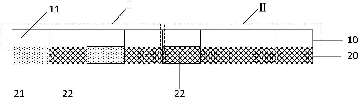
[0043] This embodiment provides a display device, such as figure 1 As shown, the display device includes a stacked driving layer 20 and a display layer 10 , wherein the driving units 21 and 22 in the driving layer 20 are electrically connected to the display units in the display layer 10 in a one-to-one correspondence.

[0044] Such as Figure 4 As shown, the driving layer 20 corresponding to the first region I is composed of driving units 21 and 22 in 4 rows and 4 columns, and the driving layer 20 corresponding to the second region II is composed of the second driving unit 22 in 4 rows and 4 columns. Corresponding to the first area I, four first driving units 21 are arranged in sequence along the horizontal direction to form a first unit row; four second driving units 22 are arranged in sequence in a horizontal direction to form a second unit row; the first unit row and The second unit rows are arranged at intervals along the vertical direction, that is, the odd-numbered row...

Embodiment 2

[0051] This embodiment provides a display device, such as Figure 5 As shown, the difference from Embodiment 1 is that: corresponding to the driving unit in the first area I, four first driving units 21 are arranged horizontally to form a continuous arrangement of first unit rows; corresponding to the driving unit in the second area II, all All the drive units are the second drive unit 22; only need to ensure that the light transmittance of the first drive unit 21 is greater than the light transmittance of the second drive unit 22, the effect of setting different drive units in different areas can be achieved. While not affecting the resolution of the display area of ​​the display device, the light transmittance of the first area I can be increased, and the fingerprint recognition rate can be improved.

[0052] As a first alternative implementation of this embodiment, corresponding to the first area I, all the driving units are all first driving units 21; corresponding to the ...

Embodiment 3

[0054] This embodiment provides a display device, such as Figure 6 As shown, the difference from Embodiment 1 or Embodiment 2 is that: along the x direction and y direction, corresponding to the driving unit in the first region I, the driving layer 20 is a first driving unit 21 and a second driving unit arranged at intervals twenty two. That is, the structures of any two adjacent driving units corresponding to the first region I are different, that is, any two adjacent driving units are the first driving unit 21 and the second driving unit 22 .

[0055] Through the first driving unit 21 and the second driving unit 22 arranged at regular intervals, the driving layer 20 corresponding to the first region I composed of 4×4 driving units is formed, so that the overall light transmission of the display device is relatively uniform, It is convenient for subsequent fingerprint identification algorithm processing.


PUM


Abstract

The invention relates to the display technical field and provides a display device. The display device comprises a display layer and a driving layer in laminated arrangement. The display layer comprises a plurality of display units in array arrangement. The driving layer comprises plurality of driving units in array arrangement. The display units and the driving units are in one-to-one correspondence and are in electrical connection. Light transmittance of the driving units is not totally same. Each element in each driving unit has metal conductivity, the metal has a certain light resistance,and light transmittance of the driving units in the driving layer is set to be not totally same, that is, a light transmitting area is formed by simplifying the structure of a drive circuit in each driving unit, so that light rays are allowed to emit out of the light transmitting area, and an effect of improving the light transmittance of the driving layer is achieved.

Description

technical field [0001] The present invention relates to the field of display technology, in particular to a display device. Background technique [0002] Organic Light Emitting Display (OLED) has self-luminescence, low driving voltage, high luminous efficiency, short response time, high definition and contrast, wide viewing angle, and can realize flexible display and large-area full-color display And many other advantages, it is recognized by the industry as the display technology with the most development potential. [0003] The active matrix OLED (English name is Active Matrix OLED, referred to as AMOLED), uses a thin film transistor (Thin Film Transistor, referred to as TFT) with a capacitor to store signals to control the brightness and grayscale performance of the OLED. Each individual OLED is electrically connected to a corresponding thin film transistor to form a pixel matrix. The array circuit formed by thin film transistors determines the light emission of the pix...

Claims


Application Information

Patent Timeline
Patent Type & Authority Applications(China)
IPC IPC(8): H01L27/32G02F1/1362
CPCG02F1/1362H10K59/121H01L27/1255G09G3/3233G09G2310/0251G09G2300/0819G09G2300/0842G09G2300/0861G09G2300/0465G06V40/1318G09G3/3225G09G3/3648
Inventor 陈心全朱修剑葛明伟王峥朱雪婧
Owner KUNSHAN GO VISIONOX OPTO ELECTRONICS CO LTD
Why Eureka
Try Eureka