


Quick Research
Generate reliable direction feasibility study reports for your R&D in just a few steps.

Technical Q&A
Discover and master advanced knowledge NOW. Basics, ideas, possibilities, all at once.

Find Solutions
As an expert in R&D theories, this can generate solutions to your technical problems instantly.

Evaluate Feasibility
Analyze your overall solution with one click, know your potential R&D risks in advance.

Monitor Landscape
Get weekly tech updates, stay abreast of the latest tech innovations and key insights.
Cavity with silicon on insulator MEMS pressure sensing device with an extended shallow polygon cavity
A technology of silicon-on-insulator and sensing devices, applied in fluid pressure measurement using changing ohmic resistance, microstructure devices composed of deformable elements, measuring fluid pressure, etc., can solve problems such as pressure sensitivity problems
- Summary
- Abstract
- Description
- Claims
- Application Information
AI Technical Summary
Problems solved by technology
Method used
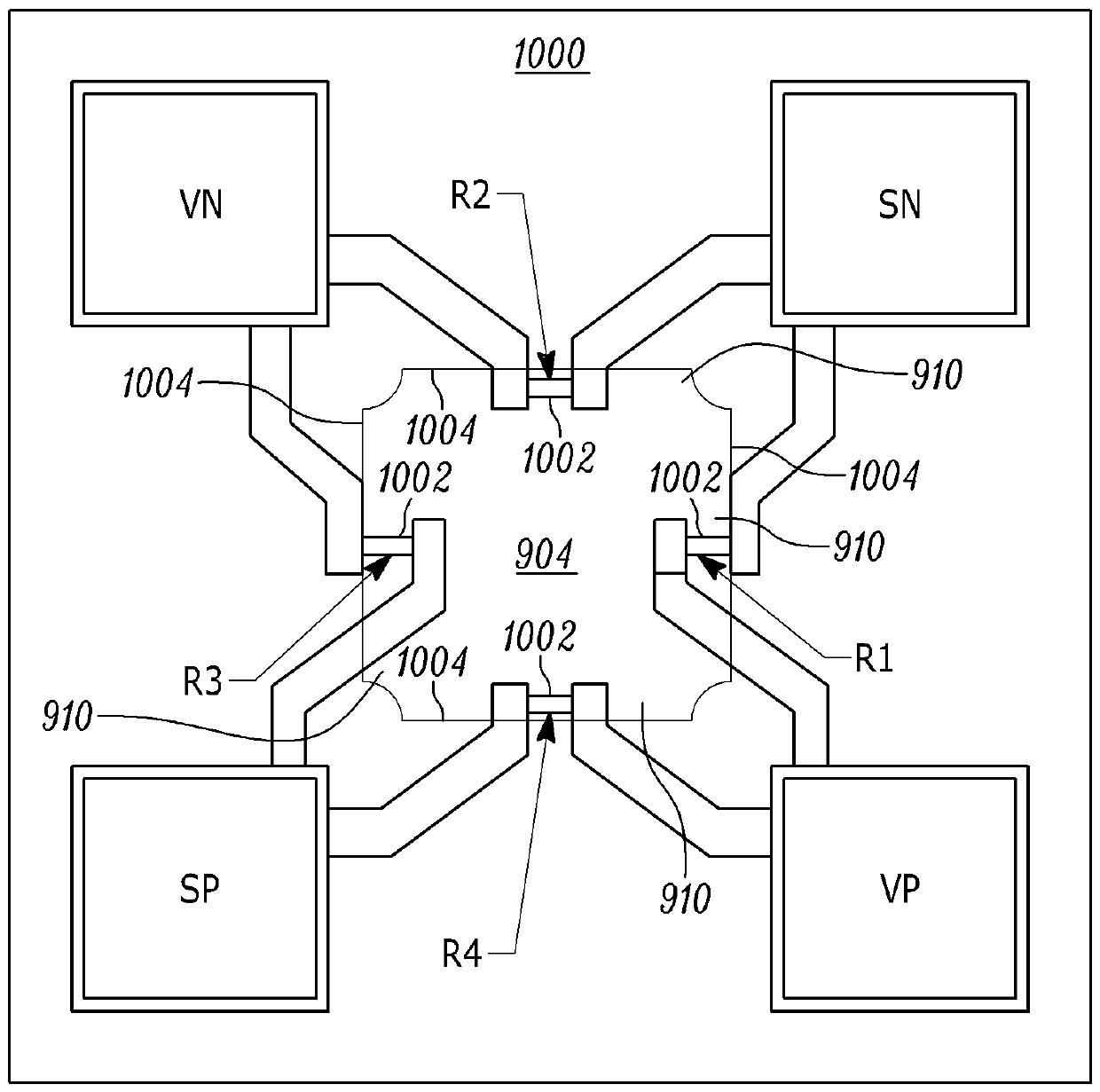
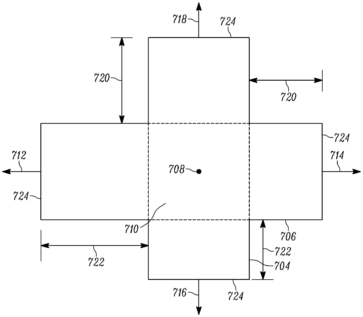
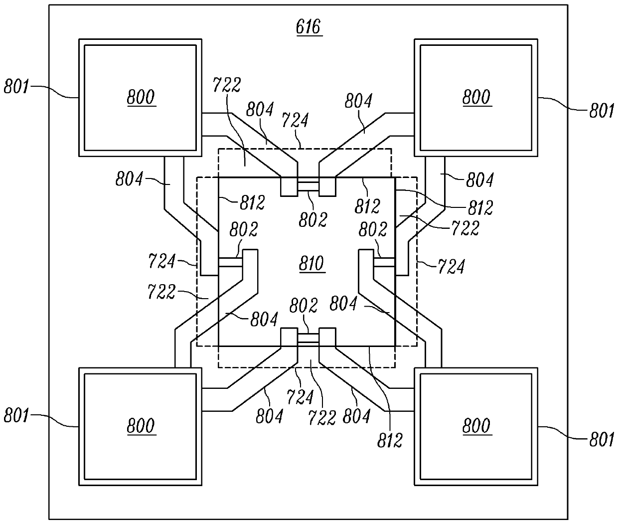
Image

Examples
Embodiment Construction
[0020] figure 1 is a perspective view of a prior art pressure sensor 100 . The pressure sensor 100 includes a plastic housing generally indicated by the reference numeral 102 .
[0021] The housing 102 has a rectangular shaped body 104, such as figure 2 The MEMS pressure sensing device 204 shown in is positioned in the rectangular shaped body 104 . Fluid (liquid or gas) pressure is applied to MEMS pressure sensing device 204 through port 106 , which extends from the outside of the housing as shown to a cavity (not shown) within housing 102 .
[0022] MEMS pressure sensing device 204 in housing 102 converts changes in fluid pressure into a voltage, which is obtained through electrical connection 108 located in a generally tubular port or port extending outwardly from housing 102 . Channel 110. In other words, pressure applied to MEMS pressure sensing device 204 within housing 102 through port 106 produces a measurable output voltage at connection terminal 108 positioned wi...
PUM
| Property | Measurement | Unit |
|---|---|---|
| thickness | aaaaa | aaaaa |
| thickness | aaaaa | aaaaa |
Abstract
Description
Claims
Application Information
 - R&D Engineer
- R&D Manager
- IP Professional
- Industry Leading Data Capabilities
- Powerful AI technology
- Patent DNA Extraction
Browse by: Latest US Patents, China's latest patents, Technical Efficacy Thesaurus, Application Domain, Technology Topic, Popular Technical Reports.
© 2024 PatSnap. All rights reserved.Legal|Privacy policy|Modern Slavery Act Transparency Statement|Sitemap|About US| Contact US: help@patsnap.com