Laser chip failure positioning analysis sample preparation method and middleware

A failure location and sample preparation technology, which is applied in the field of optical communication, can solve the problems of low chip sample sampling rate and sample preparation success rate, and achieve the effects of facilitating internal defect analysis, saving failure analysis time, and improving sampling success rate

Active Publication Date: 2018-04-10
WUHAN TELECOMM DEVICES
View PDF13 Cites 11 Cited by
  • Summary
  • Abstract
  • Description
  • Claims
  • Application Information

AI Technical Summary

Problems solved by technology

[0005] The present invention mainly solves the technical problem of low chip sample sampling rate and sample preparation success rate existing in the prior art, and provides a semiconductor laser chip failure location analysis sample preparation method and middleware

Method used


Image

  • Laser chip failure positioning analysis sample preparation method and middleware
  • Laser chip failure positioning analysis sample preparation method and middleware
  • Laser chip failure positioning analysis sample preparation method and middleware

Examples


Embodiment

[0020] The present invention will be further described below in conjunction with the accompanying drawings and examples, and those skilled in the art can easily understand other advantages and effects of the present invention from the content disclosed in this specification. The present invention can also be implemented or applied through other different specific implementation modes, and various modifications or changes can be made to the details in this specification based on different viewpoints and applications without departing from the spirit of the present invention.

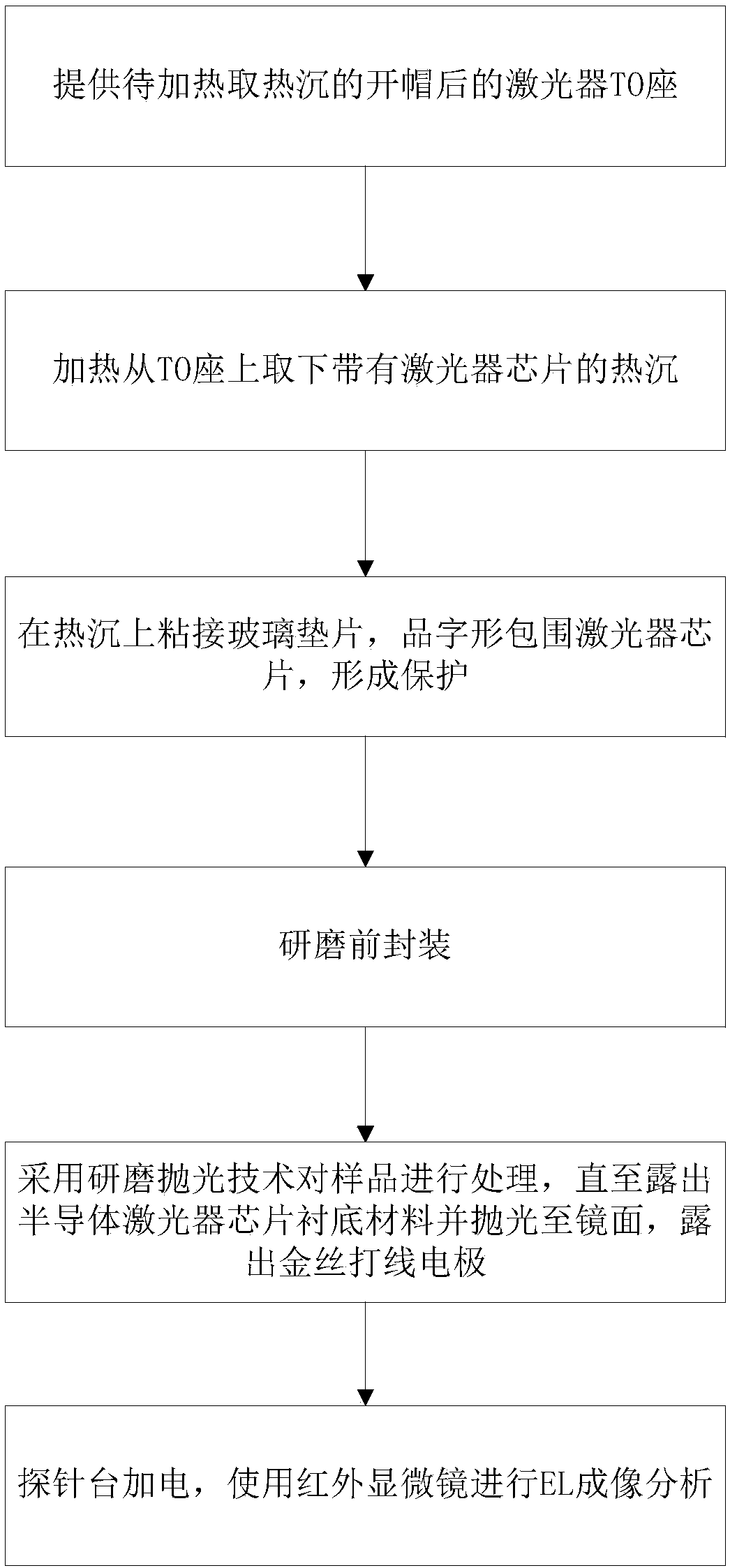
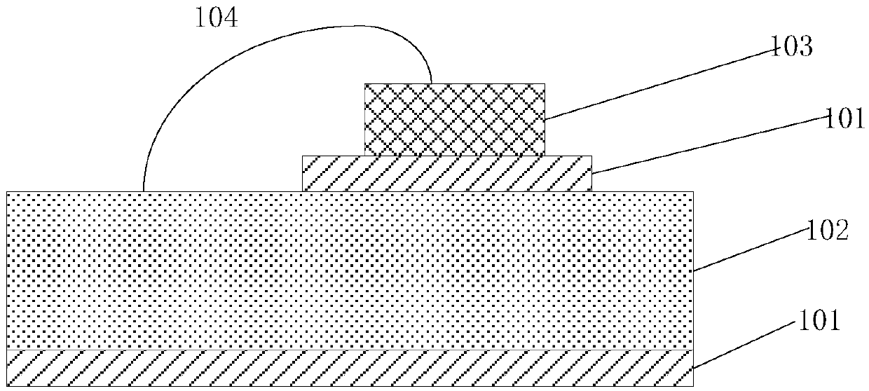
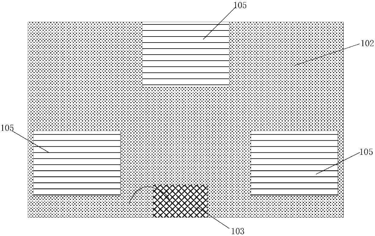
[0021] Such as Figure 1 to Figure 5 As shown, this embodiment provides a method for preparing a chip failure localization analysis sample, which at least includes the following steps:

[0022] Such as figure 1 As shown in the process flow, first perform step 1, prepare the TO of the sample to be prepared, remove the TO cap by grinding the grinding wheel, and leave the laser TO seat to be heated and take...


PUM


Abstract

The invention relates to a laser chip failure positioning analysis sample preparation method and a middleware. According to the method, the middleware and a heat sink are taken down together, foot pads for protection are bonded to the periphery of a chip, the heat sink is removed through a grinding method, and a gold layer at a substrate is removed through continuous grinding until the chip substrate is fully exposed. The method is suitable for semiconductor laser chips in multiple packaging forms, different material systems such as group IIIV, groups II and VI and silicon-based semiconductorlaser chips, can directly prepare fine and brittle laser chip samples with the scale of hundred microns, is free of precision micro-nano-processing equipment, pays attention to the protection of the samples, and can effectively prevent the damage of the sample during the failed sample taking process or during the sample preparation. Detection points are on the same plane after the sample preparation so that a power-on test is convenient. The method utilizes a cleanable adhesive and a sample can be taken out so that later analysis is promoted.

Description

technical field [0001] The invention relates to a sample preparation method and middleware, belonging to the technical field of optical communication, in particular to a laser chip failure location analysis sample preparation method and middleware. Background technique [0002] Active optical devices are the basis of optical fiber communication. With the development and wide application of optical fiber communication systems, people have higher and higher requirements for the quality and reliability of active optical devices. As the core component of active optical devices, semiconductor laser chips have stricter quality and reliability requirements. The analysis of chip failure samples has gradually penetrated into the material level. The size of semiconductor laser chips is extremely small, on the order of hundreds of um, The material properties are fragile, so it is necessary to prepare samples of failed chip samples at a scale of hundreds of um, and pay attention to prot...

Claims


Application Information

Patent Timeline
Patent Type & Authority Applications(China)
IPC IPC(8): G01N1/32
CPCG01N1/32
Inventor 黄波杨涛阙凌薇刘乔乔
Owner WUHAN TELECOMM DEVICES
Why Eureka
Try Eureka