Taiko-wafer-based wafer-level packaging structure and method

A technology of wafer-level packaging and drum wafers, which is applied in the field of wafer-level packaging structures based on Taiko wafers, and can solve problems such as unbearable process, too thin central part, and limited application of Taiko wafers.

Active Publication Date: 2018-04-13
HUATIAN TECH KUNSHAN ELECTRONICS
View PDF5 Cites 2 Cited by
  • Summary
  • Abstract
  • Description
  • Claims
  • Application Information

AI Technical Summary

Problems solved by technology

Therefore, in the manufacture of such products, after the wafer is thinned using the Taiko thinning process and the backside connection layer is made in the thinned area, if it continues to be packaged using the wafer-level packaging process, the thinned wafer The central part is too thin, and this area cannot withstand certain processes, resulting in limited application of Taiko wafers

Method used


Image

  • Taiko-wafer-based wafer-level packaging structure and method
  • Taiko-wafer-based wafer-level packaging structure and method
  • Taiko-wafer-based wafer-level packaging structure and method

Examples


Embodiment Construction

[0026] In order to make the present invention more comprehensible, the specific implementation manners of the present invention will be described in detail below in conjunction with the accompanying drawings. For convenience of description, the components in the structures in the drawings of the embodiments are not scaled according to the normal scale, so they do not represent the actual relative sizes of the structures in the embodiments.

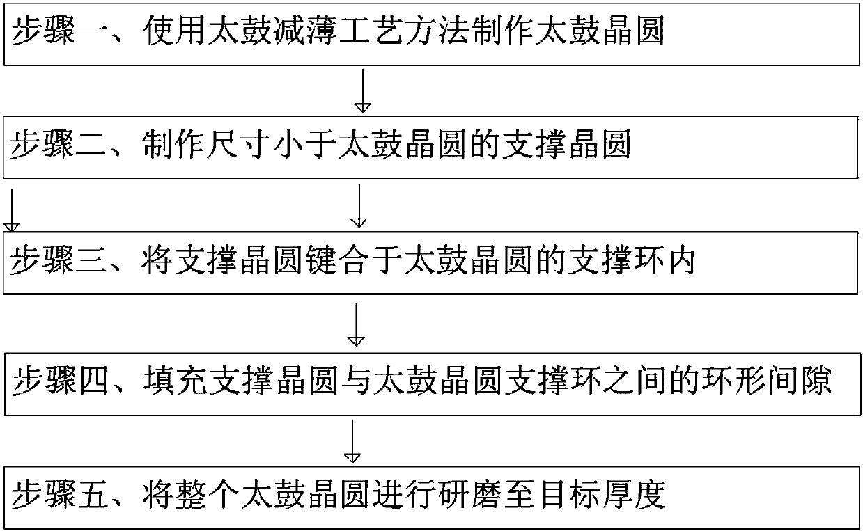
[0027] Such as figure 1 Shown is the flow chart of the method of the embodiment of the present invention, as Figure 2 to Figure 6 Shown is a schematic diagram of the wafer structure after each step in the method of the embodiment of the present invention. The wafer-level packaging method based on the Taiko wafer of the present invention comprises the following steps:

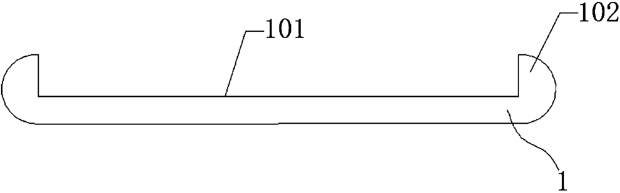
[0028] Step one, see figure 2 , using the Taiko thinning process method to thin the middle part of the back of the wafer to form a Taiko wafer 1, the middle part of the...


PUM


Abstract

The invention discloses a Taiko-wafer-based wafer-level packaging structure and method. A support wafer is arranged at the center of a Taiko wafer after reduction based on a Taiko reduction process ina bonding manner, so that thickening of the center of the Taiko wafer is realized and thus the wafer-level packaging process is carried out continuously. With the method disclosed by the invention, usage of a special Taiko wafer support ring removing device is avoided and thus the wafer-level packaging of the Taiko wafer can be realized at a standard packaging production line.

Description

technical field [0001] The invention relates to the technical field of semiconductor packaging, in particular to a wafer-level packaging structure and method based on Taiko wafers. Background technique [0002] The Taiko thinning process is a wafer thinning process developed by DISCO Corporation of Japan, and the wafers subjected to the Taiko thinning process are called Taiko wafers herein. The Taiko thinning process only thins the middle part of the wafer (silicon wafer), leaving the edge part as a support ring, and using the thinned middle part of the wafer to form an integrated circuit device, using a thicker support ring To maintain the mechanical strength of the entire wafer, prevent the wafer from curling, and facilitate the handling, transfer and processing of the wafer in the subsequent process. However, due to the existence of the support ring, the wafer-level packaging of the Taiko wafer cannot be completed in the standard packaging production line. That is to say...

Claims


Application Information

Patent Timeline
Patent Type & Authority Applications(China)
IPC IPC(8): H01L21/683
CPCH01L21/6835H01L24/94H01L2221/68327H01L2221/68377
Inventor 郑凤霞刘路路王腾马书英于大全
Owner HUATIAN TECH KUNSHAN ELECTRONICS
Why Eureka
Try Eureka