Wafer-level packaging structure and method based on Taiko wafer
A wafer-level packaging, drum wafer technology, applied in semiconductor devices, electrical components, circuits, etc., can solve problems such as too thin central part, limited application of drum wafers, and inability to withstand process processes
- Summary
- Abstract
- Description
- Claims
- Application Information
AI Technical Summary
Problems solved by technology
Method used
Image
Examples
Embodiment Construction
[0026] In order to make the present invention more comprehensible, the specific implementation manners of the present invention will be described in detail below in conjunction with the accompanying drawings. For convenience of description, the components in the structures in the drawings of the embodiments are not scaled according to the normal scale, so they do not represent the actual relative sizes of the structures in the embodiments.
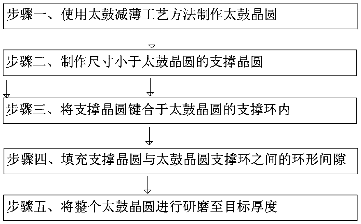
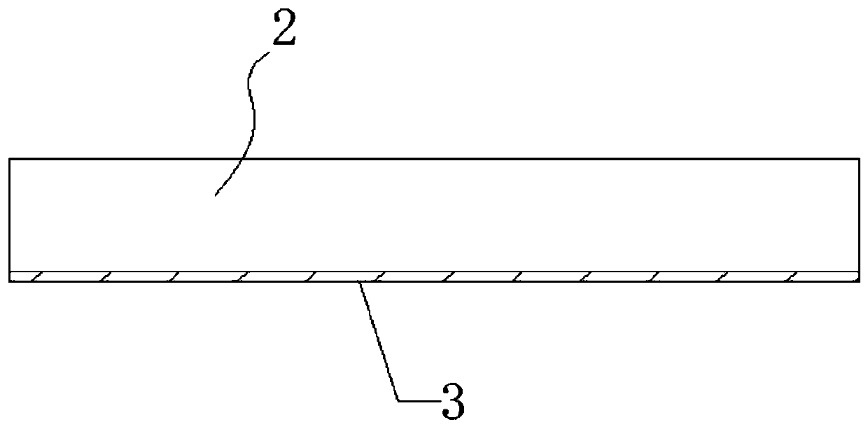
[0027] Such as figure 1 Shown is the flow chart of the method of the embodiment of the present invention, as Figure 2 to Figure 6 Shown is a schematic diagram of the wafer structure after each step in the method of the embodiment of the present invention. The wafer-level packaging method based on the Taiko wafer of the present invention comprises the following steps:
[0028] Step one, see figure 2 , using the Taiko thinning process method to thin the middle part of the back of the wafer to form a Taiko wafer 1, the middle part of the...
PUM
| Property | Measurement | Unit |
|---|---|---|
| thickness | aaaaa | aaaaa |
Abstract
Description
Claims
Application Information


