A kind of multi-layer anisotropic conductive adhesive film and its manufacturing method

A technology of anisotropic conductive adhesive and conductive adhesive layer, applied in chemical instruments and methods, layered products, electronic equipment, etc., can solve problems such as poor anisotropic conduction effect, void shielding effect, and influence on conduction performance, etc. Achieve the best oxidation resistance and conductivity, good grounding stability, and improve the effect of conduction performance

Active Publication Date: 2019-10-29
KUSN APLUS TEC CORP
View PDF4 Cites 0 Cited by
  • Summary
  • Abstract
  • Description
  • Claims
  • Application Information

AI Technical Summary

Problems solved by technology

[0002] The development trend of electronic and communication products requires circuit substrate components to develop towards light, thin, small and highly integrated, and the frequency band of transmission signals is getting wider and wider, resulting in more and more serious electromagnetic interference; at the same time, considering the safety of electronic circuit components, the electronic The grounding reliability of the circuit components in the product has put forward new requirements. Although the conductive adhesive products commonly used in the market can be connected to the grounding holes reserved in general printed circuit boards, at the same time, the grounding hole will be filled by the conductive adhesive. Too full will affect the design and installation of other components, or insufficient filling will lead to defects such as gaps in the connection part during reflow soldering and poor shielding effects. In addition, the conductive film products currently in the market are directly dispersed conductive particles in the In conductive adhesives, the conductive adhesive layer is generally thicker. If the curing is insufficient and the pressing conditions are uneven, it will lead to uneven powder distribution when the product is attached to the printed circuit board, which will affect the conduction performance. In addition, the current The metal conductive particles contained in the conductive adhesive layer are mostly spherical in shape, with a single shape, and the anisotropic conduction effect is not good

Method used


Image

  • A kind of multi-layer anisotropic conductive adhesive film and its manufacturing method
  • A kind of multi-layer anisotropic conductive adhesive film and its manufacturing method
  • A kind of multi-layer anisotropic conductive adhesive film and its manufacturing method

Examples


Embodiment

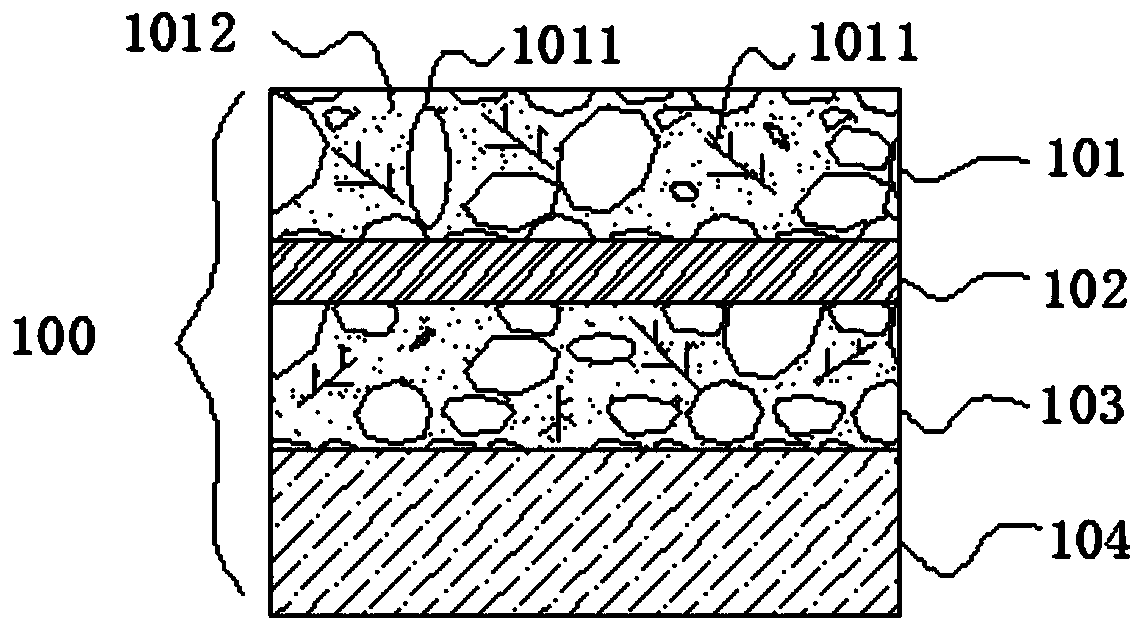
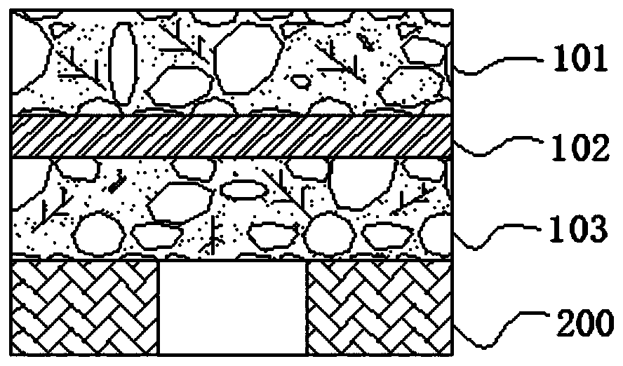
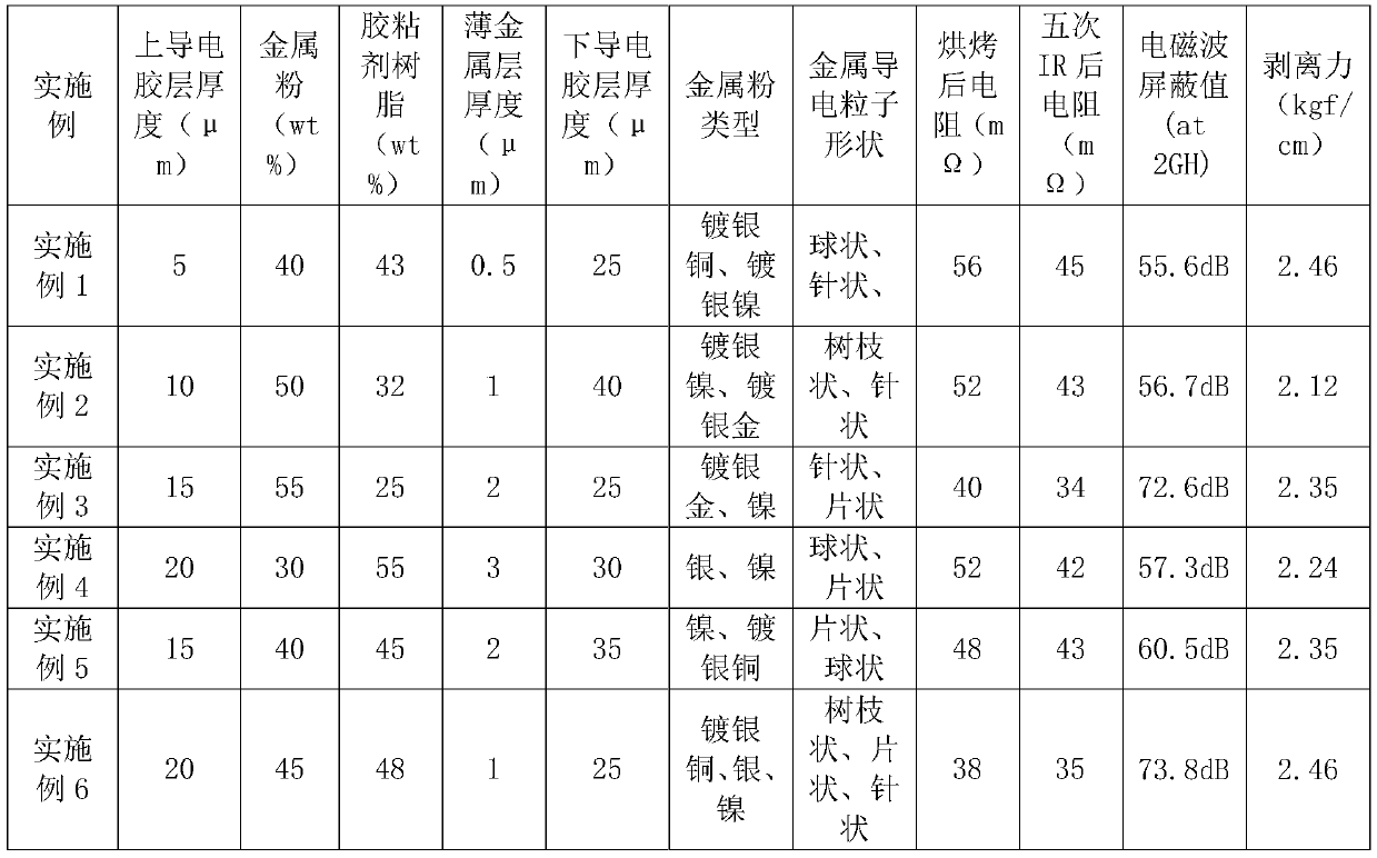
[0041] Embodiment: a kind of multi-layer anisotropic conductive adhesive film 100, such as figure 1 As shown, it includes an upper conductive adhesive layer 101, a thin metal layer 102 and a lower conductive adhesive layer 103, the thin metal layer 102 is formed between the upper conductive adhesive layer 101 and the lower conductive adhesive layer 103, the lower A release film layer or a carrier film layer 104 is formed below the conductive adhesive layer 103; the thickness of the upper conductive adhesive layer 101 is 5-20 μm, the thickness of the lower conductive adhesive layer 103 is 15-40 μm, and the thin metal The thickness of the layer 102 is 50-3000nm; the upper conductive adhesive layer 101 and the lower conductive adhesive layer 103 both include metal conductive particles 1011, and the metal conductive particles 1011 are dendritic metal powders, needle-shaped metal powders, flake-shaped At least two of metal powder and spherical metal powder, the particle diameter of...


PUM

PropertyMeasurementUnit
thicknessaaaaaaaaaa
thicknessaaaaaaaaaa
thicknessaaaaaaaaaa

Abstract

The invention discloses a multi-layer anisotropic conductive adhesive film. The multi-layer anisotropic conductive adhesive film comprises an upper conductive adhesive layer, a thin metal layer and alower conductive adhesive layer, wherein the thin metal layer is formed between the upper conductive adhesive layer and the lower conductive adhesive layer and is 50-3000 nm thick, and a release filmlayer or a carrier film layer is formed below the lower conductive adhesive layer. The multi-layer anisotropic conductive adhesive film has high conductivity and high electromagnetic wave shielding function. Metal conductive particles contained in the upper conductive adhesive layer and the lower conductive adhesive layer are in various shapes, and the thickness of the thin metal layer is nanoscale; when the conductive adhesive film is conducted, the metal conductive particles tend to flow in multiple directions, and conduction in all directions can be achieved; meanwhile, the metal conductiveparticles can pierce the thin metal layer, the number of the metal conductive particles can be reduced under the same conducting force, metal powder pollution is reduced, and the production cost is reduced.

Description

technical field [0001] The invention belongs to the technical field of conductive adhesives for printed circuit boards, and in particular relates to a multilayer anisotropic conductive adhesive film. Background technique [0002] The development trend of electronic and communication products requires circuit substrate components to develop towards light, thin, small and highly integrated, and the frequency band of transmission signals is getting wider and wider, resulting in more and more serious electromagnetic interference; at the same time, considering the safety of electronic circuit components, the electronic The grounding reliability of the circuit components in the product has put forward new requirements. Although the conductive adhesive products commonly used in the market can be connected to the grounding holes reserved in general printed circuit boards, at the same time, the grounding hole will be filled by the conductive adhesive. Too full will affect the design ...

Claims


Application Information

Patent Timeline
Patent Type & Authority Patents(China)
IPC IPC(8): B32B15/02B32B15/16B32B15/20B32B15/085B32B15/09
CPCB32B15/085B32B15/09B32B15/16B32B15/20B32B2260/025B32B2260/046B32B2307/202B32B2307/212B32B2457/00
Inventor 林志铭陈辉王影
Owner KUSN APLUS TEC CORP
Why Eureka
Try Eureka