Novel multilayer structure high-shielding electromagnetic shielding film for flexible circuit board

A technology of flexible circuit boards and electromagnetic shielding films, which is applied in the direction of circuit substrate materials, electrical components, printed circuits, etc., can solve the problems of delamination of shielding layers, rising conduction resistance, and decrease of adhesion force, etc., to achieve the best electromagnetic shielding performance , The effect of using is excellent, and the effect that meets the requirements of special conditions

Pending Publication Date: 2020-09-08
江西省信合新材料科技有限公司
View PDF7 Cites 1 Cited by
  • Summary
  • Abstract
  • Description
  • Claims
  • Application Information

AI Technical Summary

Problems solved by technology

[0004] With the advent of the 5G era, terminal products have higher and higher requirements for electromagnetic shielding films. In the future, electromagnetic shielding films will have good application prospects in high-end manufacturing fields such as mobile communications, medical displays, and military electronics; with electromagnetic shielding films The demand for electromagnetic shielding performance is getting higher and higher, and the thickness of the shielding layer will also be higher and higher, and the subsequent disadvantages will also appear, especially in the solder heat resistance of the shielding film and the simulated client SMT process test. For example, under normal conditions, after the curing process, the immersion tin test has a large area of ​​explosion, the shielding film after SMT has a large area of ​​explosion, or the conduction resistance between SMT lines has risen significantly, and at the same time, the shielding metal layer with a higher thickness is matched with a thinner insulation layer and The contact layer of conductive adhesive will cause a series of weather resistance problems, such as the obvious rise of conduction resistance under high temperature and high humidity or thermal shock test conditions, as well as the decline of adhesion force and even the delamination of the shielding layer, etc., which need to be improved

Method used


Image

  • Novel multilayer structure high-shielding electromagnetic shielding film for flexible circuit board
  • Novel multilayer structure high-shielding electromagnetic shielding film for flexible circuit board
  • Novel multilayer structure high-shielding electromagnetic shielding film for flexible circuit board

Examples


Embodiment Construction

[0035] In order to make the object, technical solution and advantages of the present invention clearer, the present invention will be further described in detail below in combination with specific embodiments and with reference to the accompanying drawings. It should be understood that these descriptions are exemplary only, and are not intended to limit the scope of the present invention. Also, in the following description, descriptions of well-known structures and techniques are omitted to avoid unnecessarily obscuring the concept of the present invention.

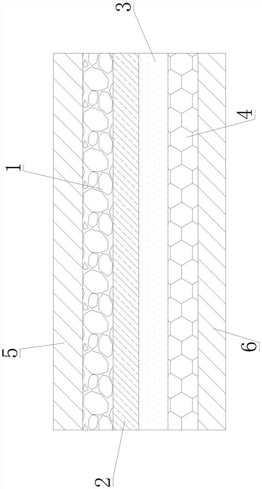
[0036] Such as figure 1 , a novel flexible circuit board proposed by the present invention has a multi-layer high shielding electromagnetic shielding film, comprising an insulating layer 1, a conductive shielding layer 2, a metal layer 3 and a conductive adhesive layer 4;

[0037] The lower surface of the insulating layer 1 is connected to the conductive shielding layer 2, the lower surface of the conductive shielding la...


PUM

PropertyMeasurementUnit
thicknessaaaaaaaaaa
thicknessaaaaaaaaaa
thicknessaaaaaaaaaa

Abstract

The invention discloses a novel multilayer structure high-shielding electromagnetic shielding film for a flexible circuit board. The shielding film comprises an insulating layer, a conductive shielding layer, a metal layer and a conductive adhesive layer; the lower surface of the insulating layer is connected to the conductive shielding layer, the lower surface of the conductive shielding layer isconnected to the metal layer, and the lower surface of the metal layer is connected to the conductive adhesive layer; wherein the total thickness of the shielding film is 10-70microm, preferably 13-38microm; the shielding film is prepared from a multi-aperture treatment copper foil; the thickness of the insulating layer is 3-25microm, preferably 5-15microm; the thickness of the conductive shielding layer is 3-10microm, preferably 3-5microm; the thickness of the metal layer is 0.1-1microm, preferably 0.2-0.5microm; and the thickness of the conductive adhesive layer is 5-20microm, preferably 10-15microm. The shielding film has excellent electromagnetic shielding performance, client SMT simulation test and SMT indicate that the conduction resistance and the heat resistance are superior to those of a common shielding film, the requirements for special conditions of a client manufacturing procedure can be effectively met, and the using effect is excellent.

Description

technical field [0001] The invention relates to the technical field of shielding films, in particular to a novel multilayer structure high shielding electromagnetic shielding film for flexible circuit boards. Background technique [0002] Under the market demand that electronic and communication products tend to be multi-functional and complex, the structure of circuit substrates needs to be lighter, thinner, shorter, and smaller, and in terms of functions, powerful and high-speed signal transmission is required. Therefore, the line density is bound to increase, the distance between the carrier board lines is getting closer and closer, and the operating frequency is moving towards high broadband. In addition, if the line layout and wiring are unreasonable, the electromagnetic interference will become more and more serious. Therefore, it is necessary to Effective management of electromagnetic compatibility, so as to maintain the normal signal transmission of electronic produc...

Claims


Application Information

Patent Timeline
Patent Type & Authority Applications(China)
IPC IPC(8): H05K1/02H05K1/05
CPCH05K1/0227H05K1/056
Inventor 周敏王振川
Owner 江西省信合新材料科技有限公司
Why Eureka
Try Eureka