Pitch change and chip scale stacking system

a chip scale and stacking technology, applied in the direction of printed circuit aspects, electrical apparatus construction details, printed circuit non-printed electric components association, etc., can solve the problems of thermal or high frequency performance problems, complex structural arrangements, and the solution of csp stacking does not address thermal gradient minimization in disclosed constructions, etc., to achieve reasonable cost

Inactive Publication Date: 2006-05-30
TAMIRAS PER PTE LTD LLC
View PDF313 Cites 139 Cited by
  • Summary
  • Abstract
  • Description
  • Claims
  • Application Information

AI Technical Summary

Problems solved by technology

The previous known methods for stacking CSPs apparently have various deficiencies including complex structural arrangements and thermal or high frequency performance issues.
Prior art, solutions to CSP stacking do not, however, address thermal gradient minimization in disclosed constructions.

Method used


Image

  • Pitch change and chip scale stacking system
  • Pitch change and chip scale stacking system
  • Pitch change and chip scale stacking system

Examples


Embodiment Construction

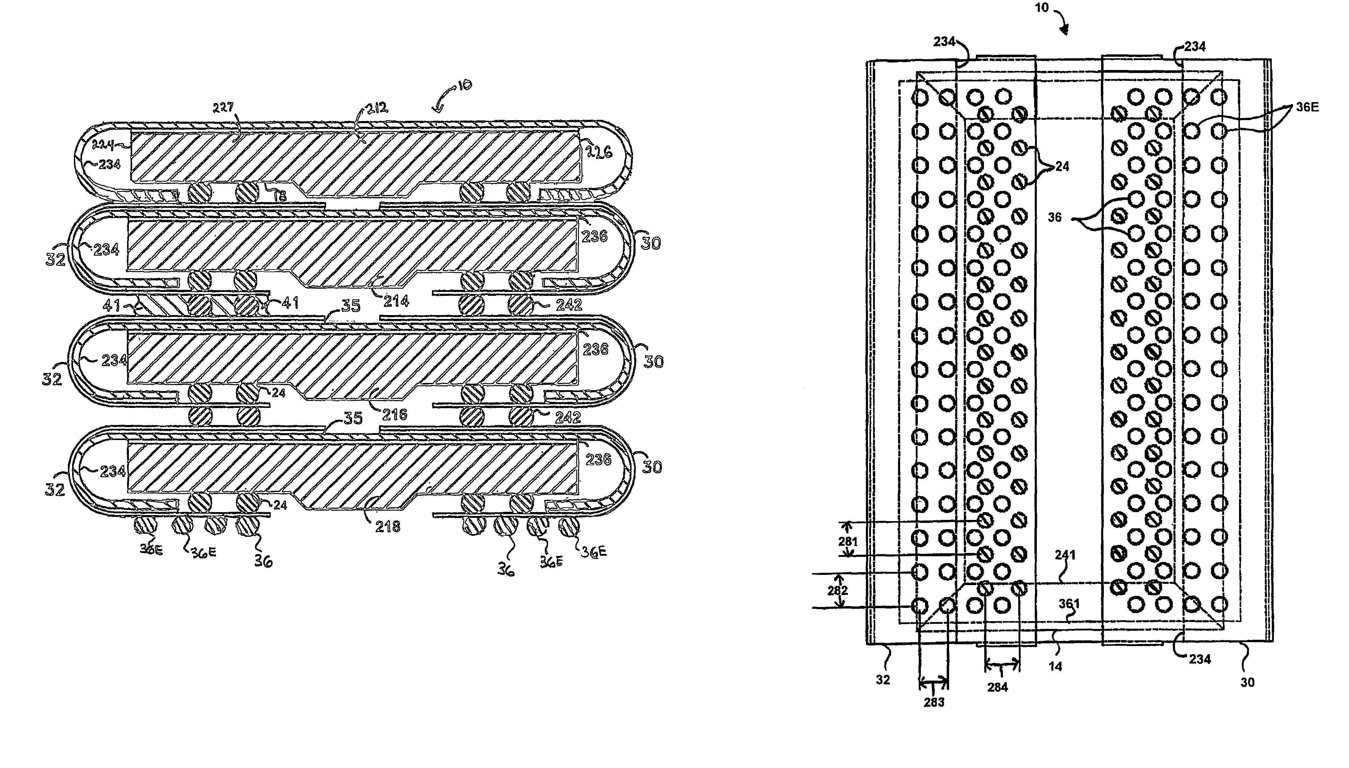
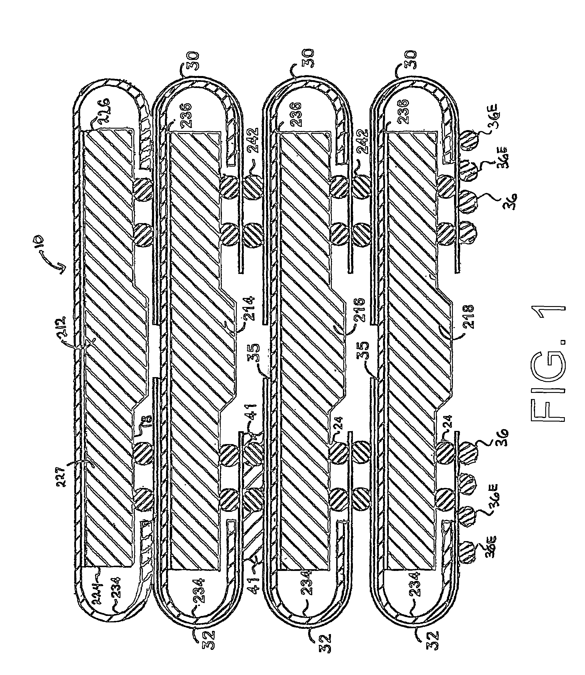
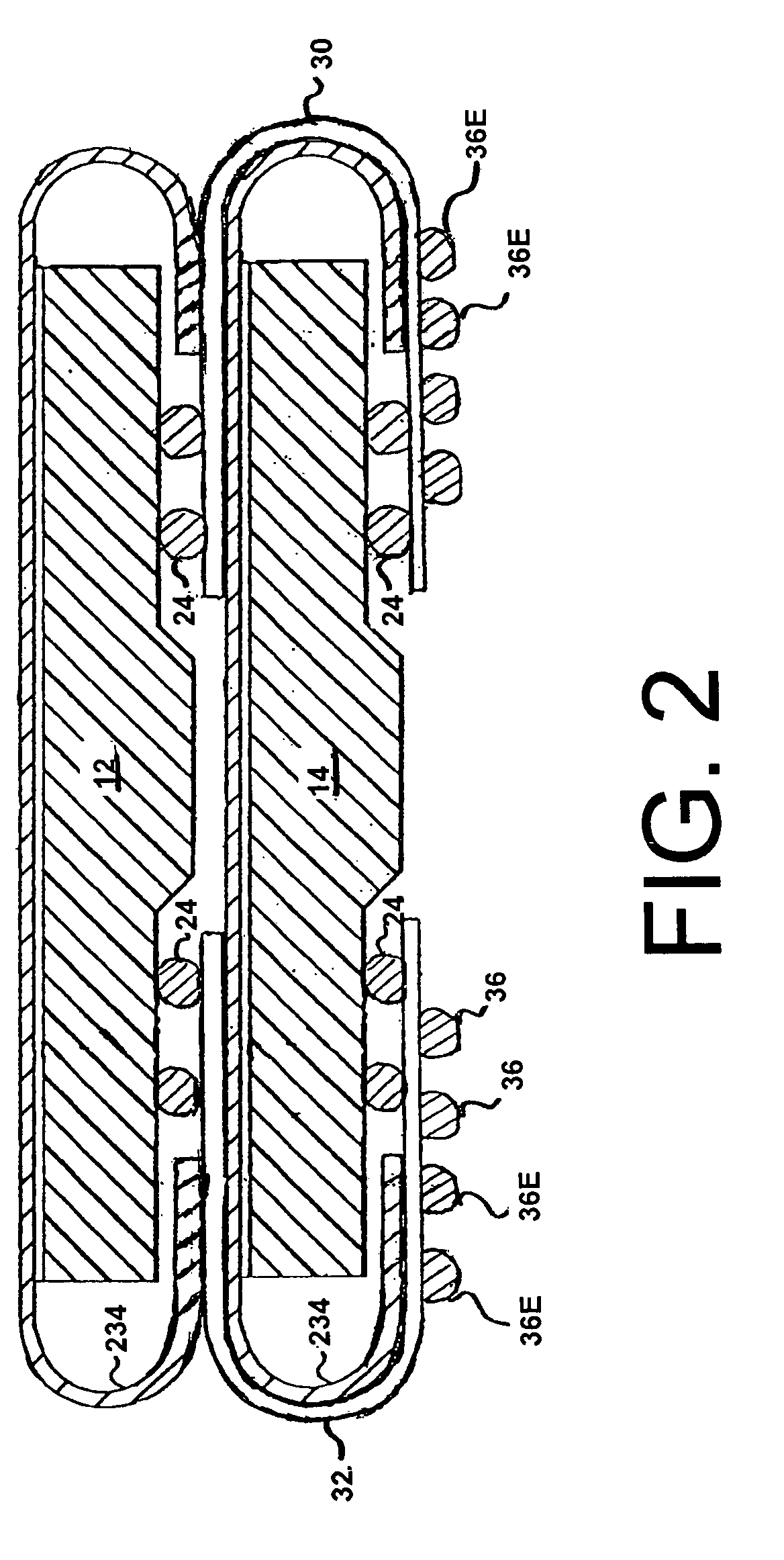
[0026]FIG. 1 is an elevation view of module 10 devised in accordance with a preferred embodiment of the present invention. Module 10 is comprised of four CSPs: level four CSP 212, level three CSP 214, level two CSP 216, and level one CSP 218. Each of the CSPs has an upper surface 16 and a lower surface 18 and opposite lateral edges 224 and 226 and typically include at least one integrated circuit surrounded by a plastic body 227. The body need not be plastic, but a large majority of packages in CSP technologies are plastic. Those of skill will realize that the present invention may be devised to create modules with different size CSPs and that the constituent CSPs may be of different types within the same module 10. For example, one of the constituent CSPs may be a typical CSP having lateral edges 224 and 226 that have an appreciable height to present a “side” while other constituent CSPs of the same module 10 may be devised in packages that have lateral edges 224 and 226 that are m...


PUM


Abstract

The present invention stacks integrated circuits into modules that conserve board surface area. In a two-high stack or module devised in accordance with a preferred embodiment of the present invention, a pair of integrated circuits is stacked, with one integrated circuit above the other. The two integrated circuits are connected with a pair of flexible circuit structures. Each of the pair of flexible circuit structures is partially wrapped about a respective opposite lateral edge of the lower integrated circuit of the module. The flex circuit pair connects the upper and lower integrated circuits and provides a thermal and electrical path connection path between the module and its application environment. The module has a ballout pattern with a different pitch and / or supplemental module contacts devised to allow combined signaling to the integrated circuits through contacts having a desired ballout footprint. The present invention may be employed to advantage in numerous configurations and combinations of integrated circuits in modules provided for high-density memories or high capacity computing.

Description

CROSS REFERENCE TO RELATED APPLICATIONS[0001]This application is a continuation-in-part of U.S. patent application Ser. No. 10 / 005,581 filed Oct. 29, 2001, now U.S. Pat. No. 6,576,992. This application is also a continuation-in-part of U.S. patent application Ser. No. 10 / 453,398, filed Jun. 3, 2003, pending, which application is a continuation-in-part of U.S. patent application Ser. No. 10 / 005,581 filed Oct. 29, 2001, now U.S. Pat. No. 6,576,992.TECHNICAL FIELD[0002]The present invention relates to aggregating integrated circuits and, in particular, to stacking integrated circuits in chip-scale packages.BACKGROUND OF THE INVENTION[0003]Leaded packages play an important role in electronics, but efforts to miniaturize electronic components and assemblies have driven development of technologies that preserve circuit board surface area. Because leaded packages have leads emergent from peripheral sides of the package, leaded packages occupy more than a minimal amount of circuit board sur...

Claims


Application Information

Patent Timeline
Patent Type & Authority Patents(United States)
IPC IPC(8): H01L23/02H01L23/31H01L23/498H01L23/538H01L25/10H05K1/14H05K1/18H05K3/36
CPCH01L23/3114H01L23/49827H01L23/4985H01L23/5387H01L25/0657H01L25/105H05K1/141H05K1/147H01L23/49816H01L2225/107H01L2224/16237H01L2225/06517H01L2225/06541H01L2225/06579H01L2225/06586H01L2924/19041H01L2924/3011H05K1/189H05K3/363H05K2201/056H05K2201/10689H05K2201/10734
Inventor ROPER, DAVID L.CADY, JAMES W.WILDER, JAMESWEHRLY, JR., JAMES DOUGLASBUCHLE, JEFFDOWDEN, JULIAN
Owner TAMIRAS PER PTE LTD LLC
Why Eureka
Try Eureka