Device for chip testing and programming and manufacturing method of device

A manufacturing method and chip testing technology, which can be applied to measuring devices, electronic circuit testing, measuring electricity, etc., can solve the problems of no large-scale use, high price, and high cost, and achieve the effect of reducing costs.

Pending Publication Date: 2018-04-20
肖敏
View PDF0 Cites 1 Cited by
  • Summary
  • Abstract
  • Description
  • Claims
  • Application Information

AI Technical Summary

Problems solved by technology

But the price of existing test or programming seat is relatively high, for example, the price of the programming seat for square flat package (QFP) chip is generally several hundred to thousands of yuan, and the cost is too high for development, so there is no need in the development process. heavily used
[0003] There is also an important shortcoming of the existing programming seat, that is, the user cannot confirm whether the programming seat is in good contact with the inserted chip.

Method used


Image

  • Device for chip testing and programming and manufacturing method of device
  • Device for chip testing and programming and manufacturing method of device
  • Device for chip testing and programming and manufacturing method of device

Examples


Embodiment Construction

[0034] In this disclosure, the various embodiments and drawings thereof are illustrative only and should not be construed in any way as limiting the scope of the disclosure. Those skilled in the art will understand that the principles of the present disclosure may be implemented in any suitable configuration or structure. Hereinafter, exemplary embodiments of the present disclosure will be described with reference to the accompanying drawings. In the following description, detailed descriptions of well-known functions or configurations will be omitted since they will unnecessarily obscure the gist of the present disclosure. Also, the terms used herein are defined according to the functions of the present disclosure. Therefore, these terms may be changed according to user's or user's intention or practice. Therefore, the terms used herein must be understood based on the description herein.

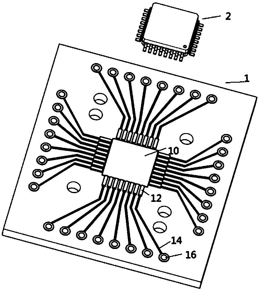
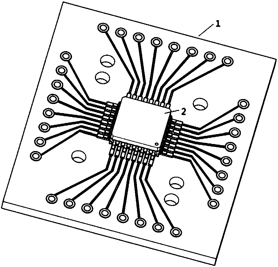
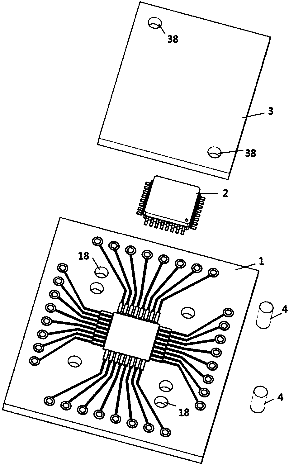
[0035] figure 1 A schematic diagram of a device for testing and programming a chip ...


PUM


Abstract

The present invention provides a device for chip testing and programming and a manufacturing method of the device. With the device for chip testing and programming and the manufacturing method of thedevice adopted, a manufacturing process can be simplified, costs can be reduced, and a user can simply confirm whether a device and a chip are in good contact. The device of the invention includes a main board; a first placement area corresponding to the main body of a chip, a plurality of first pins which surround the first placement area and are corresponding to a plurality of pins of the chip,a plurality of first contacts outside the first placement area, and a plurality of first wires, wherein each first wire connects one first pin to one first contact; and when the chip is placed on thefirst placement area, the plurality of pins of the chip are respectively contact with the plurality of first pins.

Description

technical field [0001] Embodiments of the present disclosure relate to a device for chip testing and programming and a manufacturing method thereof. Background technique [0002] Chip test sockets or programming sockets are widely used in the electronics industry. The main purpose is to write software into a large number of chips, and to perform software development and functional testing before plate making. But the price of existing test or programming seat is relatively high, for example, the price of the programming seat for square flat package (QFP) chip is generally several hundred to thousands of yuan, and the cost is too high for development, so there is no need in the development process. Used a lot. [0003] There is also an important shortcoming of the existing programming seat, that is, the user cannot confirm whether the programming seat is in good contact with the inserted chip. Contents of the invention [0004] The disclosure provides a device for chip te...

Claims


Application Information

Patent Timeline
Patent Type & Authority Applications(China)
IPC IPC(8): G01R31/28
CPCG01R31/28G01R31/2884
Inventor 肖敏
Owner 肖敏
Why Eureka
Try Eureka