Constant migration rate method for extracting source/drain parasitic resistance in nanometer MOSFET

A parasitic resistance and mobility technology, applied in electrical digital data processing, CAD circuit design, special data processing applications, etc., to achieve high accuracy, simple operation, and wide application.

Inactive Publication Date: 2018-04-20
鲁明亮
View PDF4 Cites 7 Cited by
  • Summary
  • Abstract
  • Description
  • Claims
  • Application Information

AI Technical Summary

Problems solved by technology

Therefore, how to extract the source / drain parasitic resistance in small-scale nano-CMOS devices under the condition of constant channel mobility has become a new challenge.

Method used


Image

  • Constant migration rate method for extracting source/drain parasitic resistance in nanometer MOSFET
  • Constant migration rate method for extracting source/drain parasitic resistance in nanometer MOSFET
  • Constant migration rate method for extracting source/drain parasitic resistance in nanometer MOSFET

Examples


Embodiment Construction

[0041] In order to enable those skilled in the art to better understand the technical solutions in this application, the technical solutions in this application will be clearly and completely described below in conjunction with embodiments.

[0042] Such as Figure 1-Figure 6 As shown, the present invention discloses a constant mobility method for extracting source / drain parasitic resistance in nano-MOSFET;

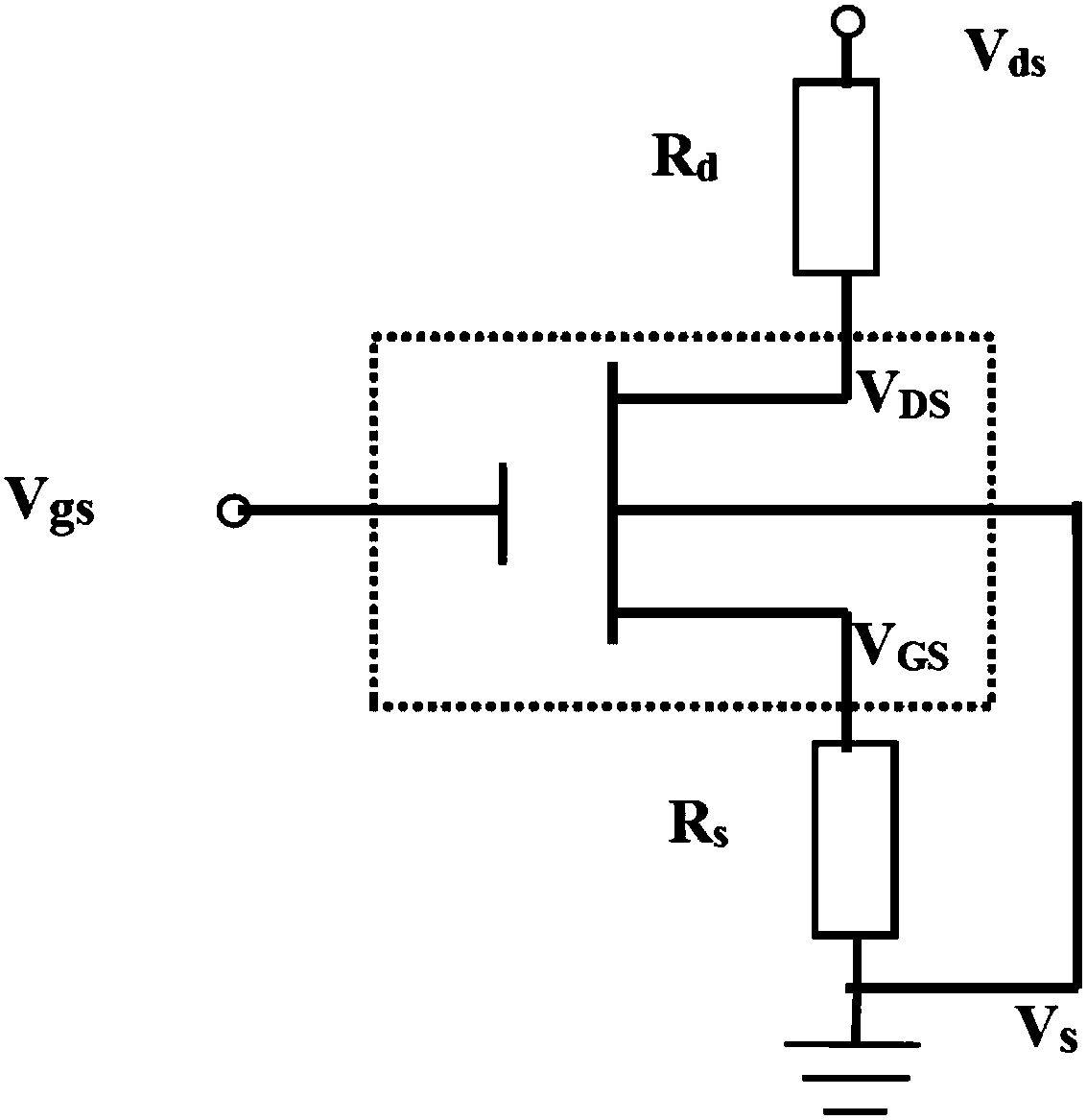
[0043] exist figure 1 Middle: V GS and V DS is the intrinsic voltage of the device circuit, V gs and V ds is the applied bias voltage of the device circuit;

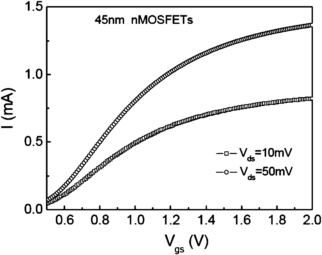
[0044] exist figure 2 Middle: The measurement conditions of the two curves are V ds = 10mV and V ds =50mV;

[0045] exist Figure 5 Middle: The points in the figure represent the R values ​​of ten samples, and the solid line is the fitting result of Weibull distribution;

[0046] exist Figure 6 Middle: V in the figure ds When taking a smaller value in the linear region, its change causes a small L ef...


PUM


Abstract

The invention discloses a constant migration rate method for extracting source/drain parasitic resistance in a nanometer MOSFET. The method comprises the following steps of (1) in a nanometer CMOS device, measuring threshold voltages VT and linear region drain currents Ids under the condition of different source and drain voltages Vds; (2) according to measurement results, selecting a proper external bias voltage condition to ensure a channel migration rate to be constant under the condition; and (3) under the proper external bias voltage condition, according to a linear region drain current Ids model, calculating out a source/drain parasitic resistance R value. According to the method, the research for parameters of the nanometer CMOS device obtains further development, and the development of reliability detection of the nanometer CMOS device is facilitated. The extraction method is high in measurement precision and is widely applied to various MOS device structures such as CMOS, SONOS, FLASH and the like; and an experimental method is simple and easy in operation.

Description

technical field [0001] The invention relates to a research on source / drain parasitic resistance of a CMOS device, in particular to a method for extracting source / drain parasitic resistance in nanometer CMOS under the condition of constant mobility. Background technique [0002] The source / drain parasitic resistance reduces the gate voltage of the intrinsic circuit ((V gs ) and drain voltage (V ds ), which reduces the driving capability of the device and is an important parameter in CMOS devices. As the size of nano-CMOS devices continues to shrink, the channel resistance (R channel ) gradually decreases, and the source / drain parasitic resistance accounts for the total device resistance (R T =R+R channel ) The proportion is getting higher and higher, which has become the main factor restricting the development of nanometer CMOS devices. Therefore, how to accurately extract the source / drain parasitic resistance of a device is a very important topic in the research of smal...

Claims


Application Information

Patent Timeline
Patent Type & Authority Applications(China)
IPC IPC(8): G06F17/50
CPCG06F30/39
Inventor 鲁明亮马丽娟
Owner 鲁明亮
Why Eureka
Try Eureka