LDMOS level shifting dv/dt noise suppression circuit for IGBT grid driver chip
A gate drive and level shifting technology, applied in electrical components, electronic switches, pulse technology, etc., can solve problems such as output waveform errors, and achieve the effects of avoiding false triggers and reducing transmission delays
- Summary
- Abstract
- Description
- Claims
- Application Information
AI Technical Summary
Problems solved by technology
Method used
Image


Examples
Embodiment Construction
[0043]The above and / or additional aspects and advantages of the present invention will become apparent and comprehensible from the following description of the embodiments in conjunction with the accompanying drawings.
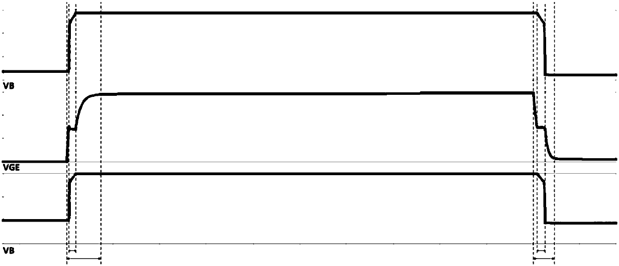
[0044] according to figure 2 The simulation waveform shows that, from the perspective of the time axis, the change of the high-side floating ground VS falls within the range of the change range of the gate voltage VGE of the IGBT to be driven. Therefore, the variation of VB caused by the variation of the high-side floating ground VS is also within the variation range of the IGBT gate voltage VGE.
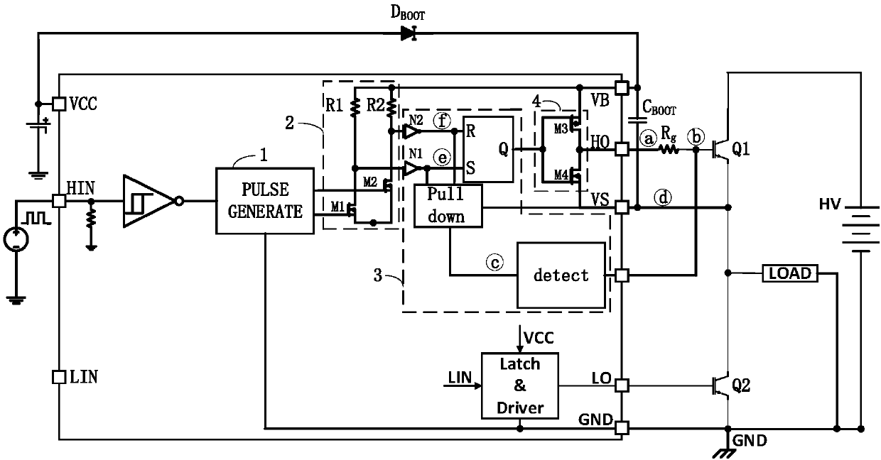
[0045] Based on the above characteristics, the present invention provides an improved LDMOS level shift dv / dt noise suppression circuit for IGBT gate drive chips. Such as image 3 As shown, the noise suppression circuit is integrated in the IGBT gate drive chip together with the low-voltage side narrow pulse generation module 1, the LDMOS level shift module 2 and...
PUM
 Abstract
Description
Claims
Application Information
 - R&D
- Intellectual Property
- Life Sciences
- Materials
- Tech Scout
- Unparalleled Data Quality
- Higher Quality Content
- 60% Fewer Hallucinations
Browse by: Latest US Patents, China's latest patents, Technical Efficacy Thesaurus, Application Domain, Technology Topic, Popular Technical Reports.
© 2025 PatSnap. All rights reserved.Legal|Privacy policy|Modern Slavery Act Transparency Statement|Sitemap|About US| Contact US: help@patsnap.com