Flip chip packaging structure and process, and camera module packaging structure

A packaging structure, flip-chip technology, applied in the direction of electrical components, electrical solid devices, circuits, etc., can solve the problems of easy damage in the process of module assembly, long delivery cycle, sensor damage, etc.

Inactive Publication Date: 2018-04-27
TRULY OPTO ELECTRONICS
View PDF6 Cites 7 Cited by
  • Summary
  • Abstract
  • Description
  • Claims
  • Application Information

AI Technical Summary

Problems solved by technology

[0003] Taking the camera module in a mobile phone as an example, in the prior art, the camera module using the Flip-chip process usually mounts the sensor, that is, the photosensitive element under the ceramic substrate, and then passes the ACF heat pressing method under the ceramic substrate. Lay flexible printed circuit board (FPC), because FPC is relatively soft, it cannot provide effective support for the back of the sensor, and the back of the module is easily affected by external forces and cause damage to the sensor; because ACF is weak in viscosity, the FPC bonded by ACF heat pressing method The pull resistance is relatively weak, so that the module cannot be p

Method used


Image

  • Flip chip packaging structure and process, and camera module packaging structure
  • Flip chip packaging structure and process, and camera module packaging structure
  • Flip chip packaging structure and process, and camera module packaging structure

Examples


Embodiment Construction

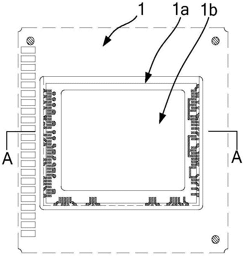
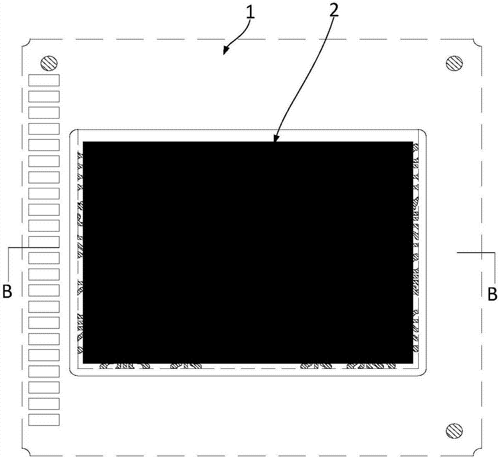
[0033] The first object of the present invention is to provide a flip-chip packaging structure, the structural design of the flip-chip packaging structure can provide effective support and protection for the sensor, has good reliability, and reduces costs. The second aspect of the present invention One purpose is to provide a flip-chip packaging process based on the above-mentioned flip-chip packaging structure and a camera module packaging structure.

[0034] The following will clearly and completely describe the technical solutions in the embodiments of the present invention with reference to the accompanying drawings in the embodiments of the present invention. Obviously, the described embodiments are only some, not all, embodiments of the present invention. Based on the embodiments of the present invention, all other embodiments obtained by persons of ordinary skill in the art without making creative efforts belong to the protection scope of the present invention.

[0035]...


PUM


Abstract

The invention discloses a flip chip packaging structure and a flip chip packaging process, and a camera module packaging structure. The flip chip packaging structure comprises a substrate, a sensor, aflexible circuit board and a plastic packaging layer, wherein a mounting groove is formed in the back surface of the substrate, the sensor is arranged in the mounting groove, the flexible circuit board is arranged on back surface of the substrate in a manner of completely or partially avoiding the mounting groove, the sensor and the flexible circuit board are electrically connected with the substrate, and the plastic packaging layer covers the mounting groove, the sensor and a connecting part of the flexible circuit board and the substrate. According to the flip chip packaging structure, theflexible circuit board completely or partially avoids the mounting groove, the plastic packaging layer is formed through injection molding into the mounting groove via a gap between the flexible circuit board and the mounting groove, effective support and protection are formed at the sensor and the joint of the flexible circuit board and the substrate by means of the plastic packaging layer, the reliability of the packaging structure is improved, and the installation difficulty is reduced, thus the substrate is no longer restricted to a ceramic substrate, thereby reducing cost of the packagingstructure, shortening the delivery cycle, and improving economic efficiency of an enterprise.

Description

technical field [0001] The invention relates to the technical field of chip packaging, in particular to a flip-chip packaging structure and process, and a camera module packaging structure. Background technique [0002] Flip-chip (Flip-Chip) packaging technology has many obvious advantages compared with the traditional wire bonding process, including superior electrical and thermal performance, high I / O pin count, package size reduction, etc., has been Widely used in LED, mobile phone manufacturing and other fields. [0003] Taking the camera module in a mobile phone as an example, in the prior art, the camera module using the Flip-chip process usually mounts the sensor, that is, the photosensitive element under the ceramic substrate, and then passes the ACF heat pressing method under the ceramic substrate. Lay flexible printed circuit board (FPC), because FPC is relatively soft, it cannot provide effective support for the back of the sensor, and the back of the module is e...

Claims


Application Information

Patent Timeline
IPC IPC(8): H01L23/31H01L21/56
CPCH01L21/56H01L23/31
Inventor 韦有兴李建华
Owner TRULY OPTO ELECTRONICS
Why Eureka
Try Eureka