

Semiconductor device
A semiconductor and device technology, applied in the field of semiconductor devices, can solve the problem that the second harmonic distortion characteristics cannot be improved, and achieve the effect of suppressing the second harmonic and improving efficiency
- Summary
- Abstract
- Description
- Claims
- Application Information
AI Technical Summary
Problems solved by technology
Method used
Image

Examples
no. 1 example
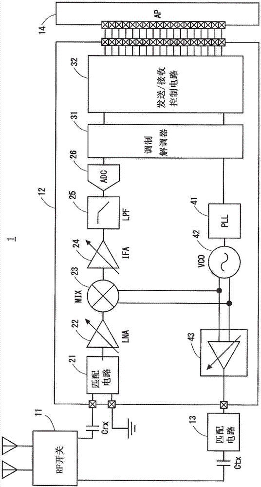
[0032] First, the semiconductor device according to the first embodiment is a radio chip that generates reception data from a reception signal input through an antenna in a communication device, and also generates a transmission signal for driving the antenna based on transmission data. Note that the semiconductor device according to the first embodiment may be in charge of one of a reception function of generating reception data from reception signals and a transmission function of generating transmission signals from transmission data in the radio chip, or may be in charge of part of the functions.
[0033] Therefore, radio equipment including the semiconductor device according to the first embodiment is explained hereinafter. figure 1 is a block diagram of the radio device 1 according to the first embodiment. Please be aware of, figure 1 The radio configurations shown in are examples of radio configurations only. That is, the circuitry used to implement a radio is not lim...
no. 2 example
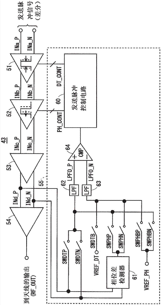
[0130] In the second embodiment, a power amplifier unit 43a is explained as another embodiment of the power amplifier unit 43 according to the first embodiment. In the description of the second embodiment, the same symbols as those in the first embodiment are assigned to the same components as those in the first embodiment, and descriptions thereof are omitted.
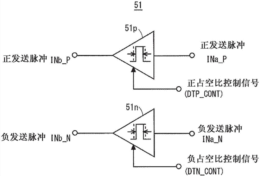
[0131] Figure 18 A block diagram of a power amplifier unit 43a of the semiconductor device according to the second embodiment is shown. Such as Figure 18 As shown in , the power amplifier unit 43a according to the second embodiment is obtained by the following steps: In the power amplifier unit 43 according to the first embodiment, the duty ratio adjustment circuit 51 is removed, and the phase difference setting circuit 75 and the transmission The pulse control circuit 80 replaces the phase difference setting circuit 55 and the transmission pulse control circuit 60, respectively. The phase difference setting circ...
PUM
 Abstract
Description
Claims
Application Information