A kind of Gan-based heterojunction diode and its preparation method

A heterojunction and diode technology, applied in the direction of diodes, semiconductor/solid-state device manufacturing, semiconductor devices, etc., can solve the problems of large reverse leakage current, cannot be adjusted, and cannot effectively reduce the reverse leakage current of devices, and achieve low turn-on voltage, high reliability, and low reverse leakage current effects

Active Publication Date: 2021-02-02
INST OF SEMICONDUCTORS - CHINESE ACAD OF SCI +1
View PDF5 Cites 0 Cited by
  • Summary
  • Abstract
  • Description
  • Claims
  • Application Information

AI Technical Summary

Problems solved by technology

Due to the limitation of the Schottky barrier of conventional GaN Schottky diodes, the forward turn-on voltage is generally fixed at about 1V and cannot be adjusted.
[0006] 2. Large reverse leakage current
[0007] In response to these shortcomings, the researchers proposed to use high and low work function metal layer mixed anodes, F ion implantation technology under the Schottky, and groove anodes to make Schottky diodes, which can effectively reduce the turn-on voltage of Schottky diodes. However, it cannot effectively reduce the reverse leakage current of the device, effectively reduce the turn-on voltage and reverse leakage current of GaN diodes, and increase the breakdown voltage has become the main problem to be solved.

Method used


Image

  • A kind of Gan-based heterojunction diode and its preparation method
  • A kind of Gan-based heterojunction diode and its preparation method
  • A kind of Gan-based heterojunction diode and its preparation method

Examples


Embodiment Construction

[0025] In order to make the object, technical solution and advantages of the present invention clearer, the present invention will be described in further detail below in conjunction with specific embodiments and with reference to the accompanying drawings.

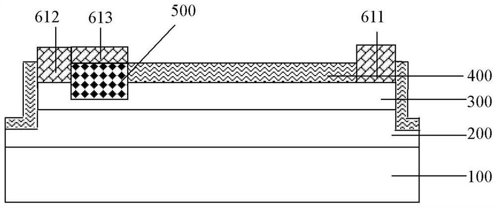
[0026] figure 1 It is a schematic structural diagram of a GaN-based heterojunction diode according to an embodiment of the present invention, such as figure 1 As shown, in an embodiment of the present invention, the GaN-based heterojunction diode includes:

[0027] A substrate 100, the substrate 100 may be a substrate material such as GaN, sapphire, Si, diamond or SiC;

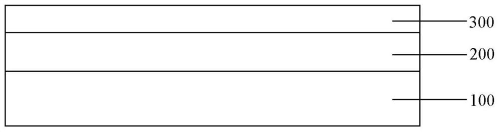
[0028] a GaN intrinsic layer 200 formed on the substrate 100, wherein the thickness of the GaN intrinsic layer 200 is 50 nm-10 μm;

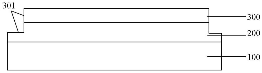
[0029] The barrier layer 300 is formed on the GaN intrinsic layer 200, and a mesa pattern is formed on the barrier layer 300 and the GaN intrinsic layer 200 to isolate from other GaN diodes, the height of the mesa pattern ...


PUM

PropertyMeasurementUnit
thicknessaaaaaaaaaa
thicknessaaaaaaaaaa
thicknessaaaaaaaaaa

Abstract

The invention discloses a GaN-based heterojunction diode and a preparation method thereof. The GaN-based heterojunction diode comprises: a GaN intrinsic layer and a barrier layer grown sequentially on a substrate; In the groove area, the high hole concentration structure layer covers the upper surface of the groove; the cathode electrode is located on the part of the upper surface of the barrier layer that is not covered by the high hole concentration structure layer; the first part of the anode electrode is located on the upper surface of the barrier layer and is not covered by the high hole concentration layer. Another part of the area covered by the concentration structure layer is located next to the high hole concentration structure layer; the second part of the anode electrode covers the upper surface of the high hole concentration structure layer; the passivation protection layer covers the upper surface of the barrier layer and is not covered by the cathode The area covered by electrodes and anode electrodes. The invention has high reliability and good repeatability, can realize the adjustment of the opening voltage of the device, and obtains a GaN heterojunction diode with low opening voltage and low reverse leakage current.

Description

technical field [0001] The invention relates to the technical field of manufacturing semiconductor devices, in particular to a GaN-based heterojunction diode with a p-type multi-component nitride alloy with a gradual change in composition added to a GaN heterojunction structure and a preparation method thereof. Background technique [0002] GaN material has unique advantages in the preparation of high-voltage, high-temperature, high-power and high-density integrated electronic devices because of its large band gap, high critical breakdown electric field, and high thermal conductivity. [0003] GaN materials can form heterojunction structures with AlGaN, InAlN and other materials. Due to the spontaneous polarization and piezoelectric polarization effects of materials such as AlGaN or InAlN, a high-concentration and high-mobility two-dimensional electron gas (2DEG) will be formed at the heterojunction interface. This characteristic can not only improve the carrier mobility an...

Claims


Application Information

Patent Timeline
Patent Type & Authority Patents(China)
IPC IPC(8): H01L29/861H01L29/06H01L21/329
CPCH01L29/0619H01L29/66219H01L29/861
Inventor 梁亚楠贾利芳何志樊中朝颜伟杨富华
Owner INST OF SEMICONDUCTORS - CHINESE ACAD OF SCI
Why Eureka
Try Eureka