Trench type super junction and method of making the same

A manufacturing method and super junction technology, which is applied in semiconductor/solid-state device manufacturing, semiconductor devices, electrical components, etc., can solve problems such as poor uniformity of reverse breakdown voltage, and achieve the effect of improving in-plane uniformity

Active Publication Date: 2020-08-07
SHANGHAI HUAHONG GRACE SEMICON MFG CORP
View PDF8 Cites 0 Cited by
  • Summary
  • Abstract
  • Description
  • Claims
  • Application Information

AI Technical Summary

Problems solved by technology

In the etching of trenches, the morphology of trenches in different regions of the same semiconductor substrate is not exactly the same, and the reverse breakdown voltage of super junction devices is greatly affected by the morphology of trenches, making the same crystal The uniformity of the reverse breakdown voltage of the super junction device on the circle is poor

Method used


Image

  • Trench type super junction and method of making the same
  • Trench type super junction and method of making the same
  • Trench type super junction and method of making the same

Examples


Embodiment Construction

[0050] Before describing the embodiments of the present invention, the influence of process mismatch on the breakdown voltage of existing trench-type super junction devices is introduced first:

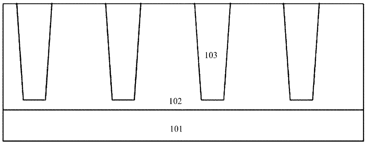
[0051] Such as figure 1 As shown, it is a schematic structural diagram of an existing groove-type super junction; an N-type epitaxial layer 102 is formed on the surface of an N-type semiconductor substrate such as a silicon substrate 101, and a plurality of trenches are formed in the N-type epitaxial layer 102. Each trench is filled with a P-type epitaxial layer 103, and the P-type epitaxial layer 103 filled in each trench forms a P-type thin layer, that is, a P-type column 103, and the N-type epitaxial layer between each P-type thin layer 103 Layer 102 constitutes an N-type thin layer. figure 1 The structure shown shows that the super junction is composed of a plurality of N-type thin layers and P-type thin layers 103 arranged alternately. figure 1 shows an alternate arrangement of...


PUM


Abstract

The invention discloses a trench type super junction. The trench type super junction comprises a plurality of trenches formed in a first conductive type first epitaxial layer, wherein each trench is filled with a second conductive type second epitaxial layer which is not full of the trench; the gaps of the trenches are fully filled with first conductive type third epitaxial layers; and the sizes of the second epitaxial layers of respective super junction units are the same, while the sizes of the first epitaxial layers and the third epitaxial layers are also the same, so that the sum of the total doping amount of the first conductive type of the first and third epitaxial layers in the respective super junction units is matched with the sum of the total doping amount of the second conductive type of the second epitaxial layers. The invention also discloses a manufacturing method of the trench type super junction. Charge matching of respective super junction units can be realized in a self-alignment manner, in-plane uniformity of the reverse breakdown voltage of a super junction device can be improved, and the process window range of the reverse breakdown voltage can be enlarged.

Description

technical field [0001] The invention relates to the field of semiconductor integrated circuit manufacturing, in particular to a trench super junction; the invention also relates to a method for manufacturing the trench super junction. Background technique [0002] The super junction is composed of alternately arranged P-type thin layers (also called P-type pillars) and N-type thin layers (also called N-type pillars) formed in a semiconductor substrate, and the matching is completed by using P-type thin layers and N-type thin layers The formed depletion layer supports the reverse withstand voltage while maintaining a small on-resistance. [0003] The pillar structure of the PN interval of the super junction is the biggest feature of the super junction. Currently, there are mainly two methods for manufacturing the pillar structure of the PN spacer, one is obtained by multiple epitaxy and ion implantation, and the other is made by deep trench etching and epitaxy (EPI) filling....

Claims


Application Information

Patent Timeline
Patent Type & Authority Patents(China)
IPC IPC(8): H01L27/04H01L29/06H01L21/822
CPCH01L21/822H01L27/04H01L29/0634
Inventor 孔蔚然李昊
Owner SHANGHAI HUAHONG GRACE SEMICON MFG CORP
Why Eureka
Try Eureka