Wafer processing device and system for automatically measuring wafer bonding energy

A technology for processing devices and wafers, applied in semiconductor/solid-state device testing/measurement, electrical components, circuits, etc., can solve problems such as inaccuracy, excessive deviation of bonding energy measurement values, uneven insertion speed, etc., and achieve measurement Accurate value, good repeatability, and the effect of eliminating errors

Inactive Publication Date: 2018-05-15
HUAIAN IMAGING DEVICE MFGR CORP
View PDF3 Cites 10 Cited by
  • Summary
  • Abstract
  • Description
  • Claims
  • Application Information

AI Technical Summary

Problems solved by technology

This method of manually inserting sheets and measuring manually is highly influenced by human factors
For example, the speed of insertion and the force used when manually inserting sheets may be non-uniform, making the resulting crack length not an accurate reflection of the bonding energy between wafers
Also, the visual reading of the crack length measurement by the operator can cause large discrepancies
Therefore, manual sheet insertion and manual measurement can easily lead to excessive deviations in the bonding energy measurement
Inaccurate bond energy measurements can easily lead to wafer slippage or cracking during subsequent wafer processing
In addition, manual measurement methods are inefficient and poorly repeatable, making them unsuitable for scenarios requiring multiple measurements
Also, the operator is vulnerable to injury from the sheet

Method used


Image

  • Wafer processing device and system for automatically measuring wafer bonding energy
  • Wafer processing device and system for automatically measuring wafer bonding energy
  • Wafer processing device and system for automatically measuring wafer bonding energy

Examples


Embodiment Construction

[0020] Various exemplary embodiments of the present disclosure will now be described in detail with reference to the accompanying drawings. It should be noted that relative arrangements of components and steps, numerical expressions and numerical values ​​set forth in these embodiments do not limit the scope of the present disclosure unless specifically stated otherwise.

[0021] The following description of at least one exemplary embodiment is merely illustrative in nature and in no way intended as any limitation of the disclosure, its application or uses.

[0022] Techniques, methods and devices known to those of ordinary skill in the relevant art may not be discussed in detail, but where appropriate, such techniques, methods and devices should be considered part of the Authorized Specification.

[0023] In all examples shown and discussed herein, any specific values ​​should be construed as illustrative only, and not as limiting. Therefore, other examples of the exemplary ...


PUM


Abstract

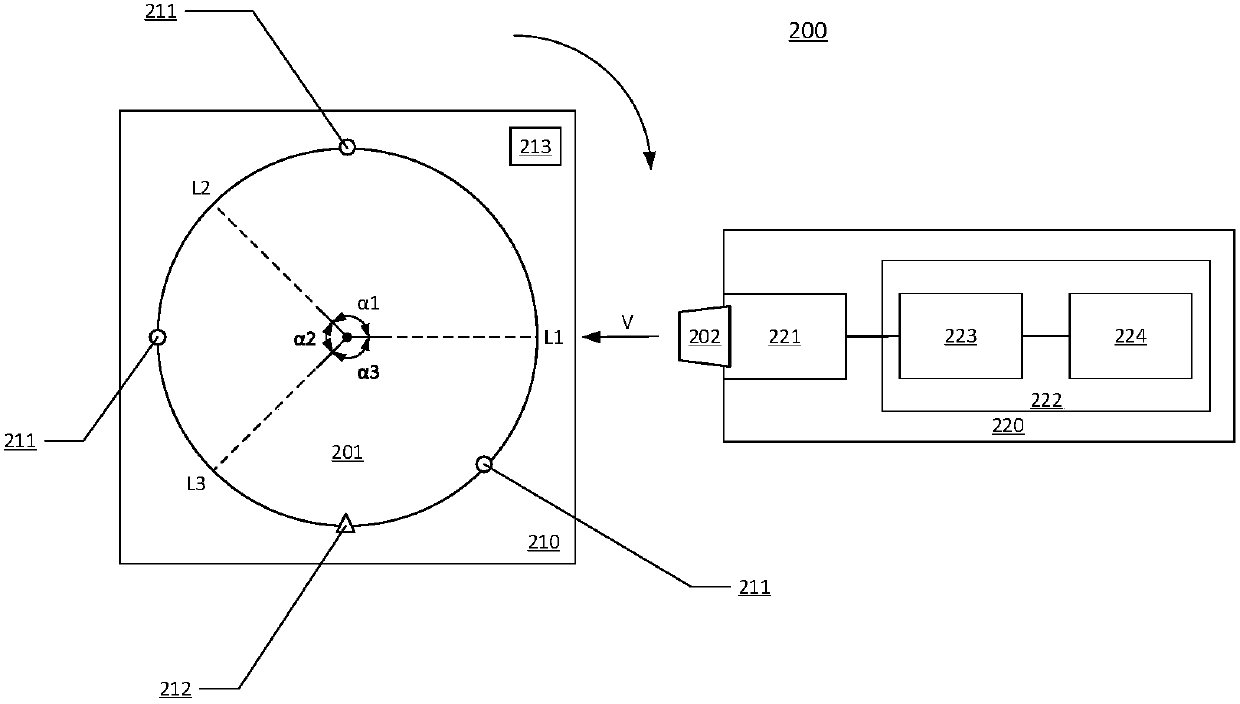
The invention relates to a wafer processing device and a system for automatically measuring the wafer bonding energy. One embodiment relates to a wafer processing device which includes a wafer fixingmechanism used for fixing bonded wafers and a sheet inserting mechanism used for inserting a sheet between the bonded wafers. The sheet inserting mechanism includes a sheet fixing mechanism and a sheet driving mechanism. A sheet is fixedly installed at one end of the sheet fixing mechanism near the wafer fixing mechanism. The sheet driving mechanism is coupled to the sheet fixing mechanism, and isconfigured to drive the sheet fixing mechanism to move towards the wafer fixing mechanism so that the sheet can be inserted in an alignment manner between the bonded wafers at a preset uniform speed.

Description

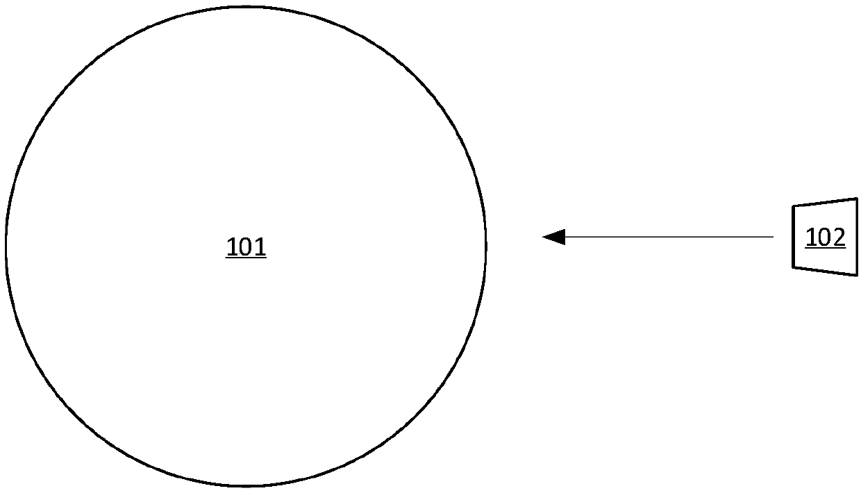
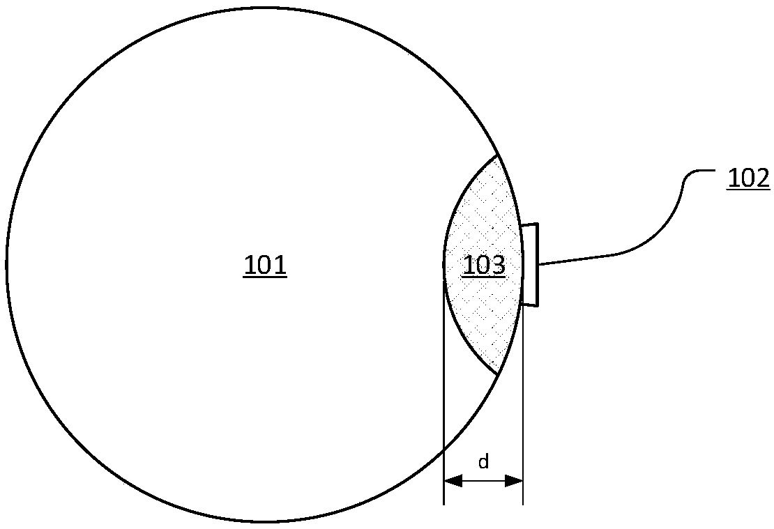
technical field [0001] The present disclosure relates to the field of semiconductors, in particular, to a wafer processing device and a system for automatically measuring wafer bonding energy. Background technique [0002] In a semiconductor manufacturing process such as a back-illuminated image sensor manufacturing process, it is necessary to bond two or more wafers together and measure the bonding energy between the bonded wafers. One way to measure bonding energy is to insert a thin sheet between the bonded wafers and measure the length of the crack on the resulting wafer. This crack length can reflect the magnitude of the bonding energy between the bonded wafers. [0003] Usually, the above-mentioned method of measuring bonding energy is performed manually by an operator. That is, the sheet is manually inserted between the bonded wafers by the operator, and the length of the crack generated on the wafer is manually measured by the operator using a ruler. This method o...

Claims


Application Information

Patent Timeline
Patent Type & Authority Applications(China)
IPC IPC(8): H01L21/66
CPCH01L22/12
Inventor 吕新强田得暄林宗贤吴龙江郭松辉王海宽
Owner HUAIAN IMAGING DEVICE MFGR CORP
Why Eureka
Try Eureka