Method and system of releasing a MEMS structure

a mems and structure technology, applied in the field of mems structure, can solve the problems of high non-standard packaging, and general fragility of the mems feature, and achieve the effect of reducing the cost of many mems devices and reducing the risk of damag

Active Publication Date: 2007-07-31
INVENSENSE
View PDF7 Cites 143 Cited by
  • Summary
  • Abstract
  • Description
  • Claims
  • Application Information

AI Technical Summary

Problems solved by technology

MEMS features are generally very fragile and sensitive to dusts and particles.
Such non-standard packaging has been primary contributor to the inherent high cost of many MEMS devices.
However, one of the key challenges in performing any of the protective capping techniques has been to allow for easy access to the input / output pads.
However, this requires added processing and the etching through the wafers.
There are several limitations to this method.
First, the number of openings per device are fairly limited due to mechanical limitations and wafer fragility in case of many openings.
Secondly, the openings can not be continuous on any one side.
Etching a hole through a wafer has its challenges and requires careful design and process development.
The disadvantage of this method is that all materials present on the wafer must either be compatible (i.e., not etch) or they must be protected.
The number of compatible materials is limited, particularly if the release takes a significant amount of time.
Protecting incompatible materials requires an additional process step, and often creates process compatibility issues of its own.
Finally, another disadvantage of this method is the difficulty in masking this etch.
For long, through-wafer etching, the number of materials that can be effectively patterned as a mask are quite limited.
Etching through 400 to 500 microns of silicon cover can take a significant amount of time and is also a fairly costly process.
However, a DRIE system is costly, requiring significant capital expenditure.
Furthermore, a DRIE process is time consuming when removing significant (>200 μm) amount of silicon.
Accordingly, the throughput of the machine utilized for etching is significantly limited.
Dry etching requires patterning a masking material to define the feature(s) to be released, similar to wet etching, and has the same problems associated therewith.
The problem with this approach is that it is difficult to control the depth of the saw into the cover wafer accurately.
In addition, removal of the unwanted silicon tabs after sawing is often destructive and potentially damaging.
Alternatively, a clearing channel can be etched into the cover wafer to allow for sawing operation, but this is also problematic.
Since the saw slurry will get under the silicon and over the contact pads which results in poor contact and wire bond assembly.
Also, having large pieces of silicon tabs flying off the wafers during the saw operation is not considered standard and often results in damage to the saw blades.

Method used


Image

  • Method and system of releasing a MEMS structure
  • Method and system of releasing a MEMS structure
  • Method and system of releasing a MEMS structure

Examples


Embodiment Construction

[0023]The present invention relates generally to a MEMS structure and more specifically to a method and system for releasing such a structure after manufacturing. The following description is presented to enable one of ordinary skill in the art to make and use the invention and is provided in the context of a patent application and its requirements. Various modifications to the preferred embodiments and the generic principles and features described herein will be readily apparent to those skilled in the art. Thus, the present invention is not intended to be limited to the embodiments shown, but is to be accorded the widest scope consistent with the principles and features described herein.

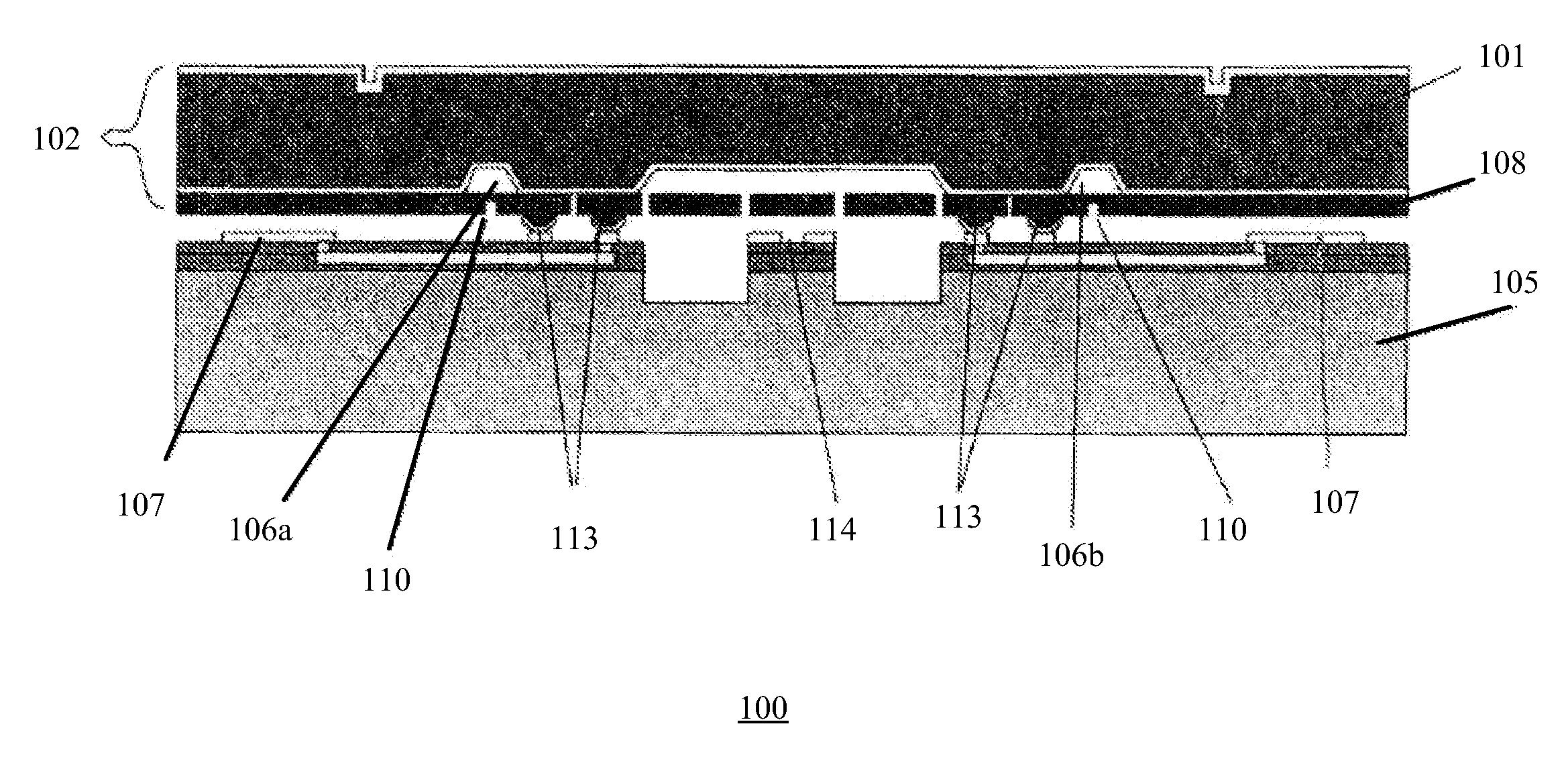
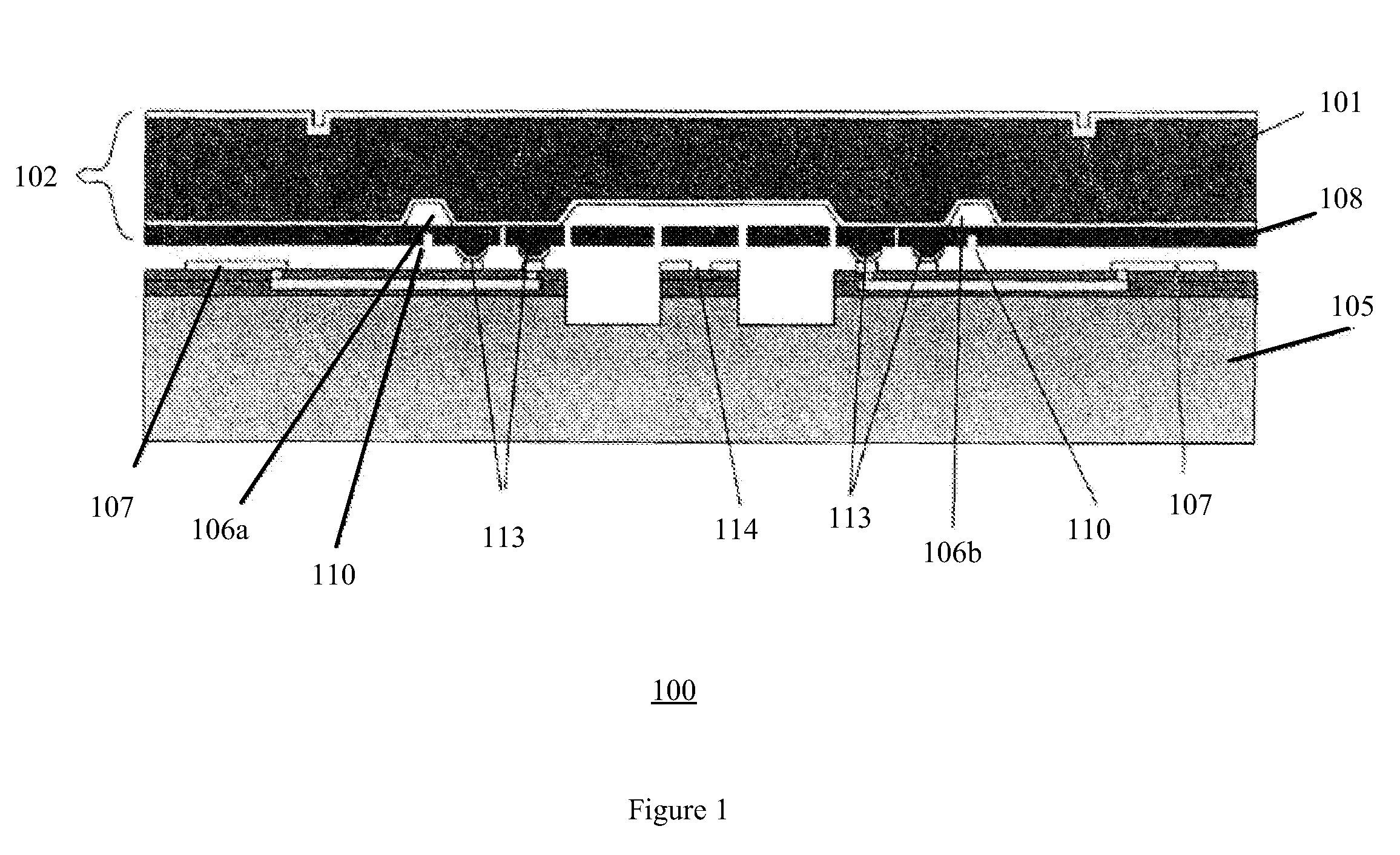
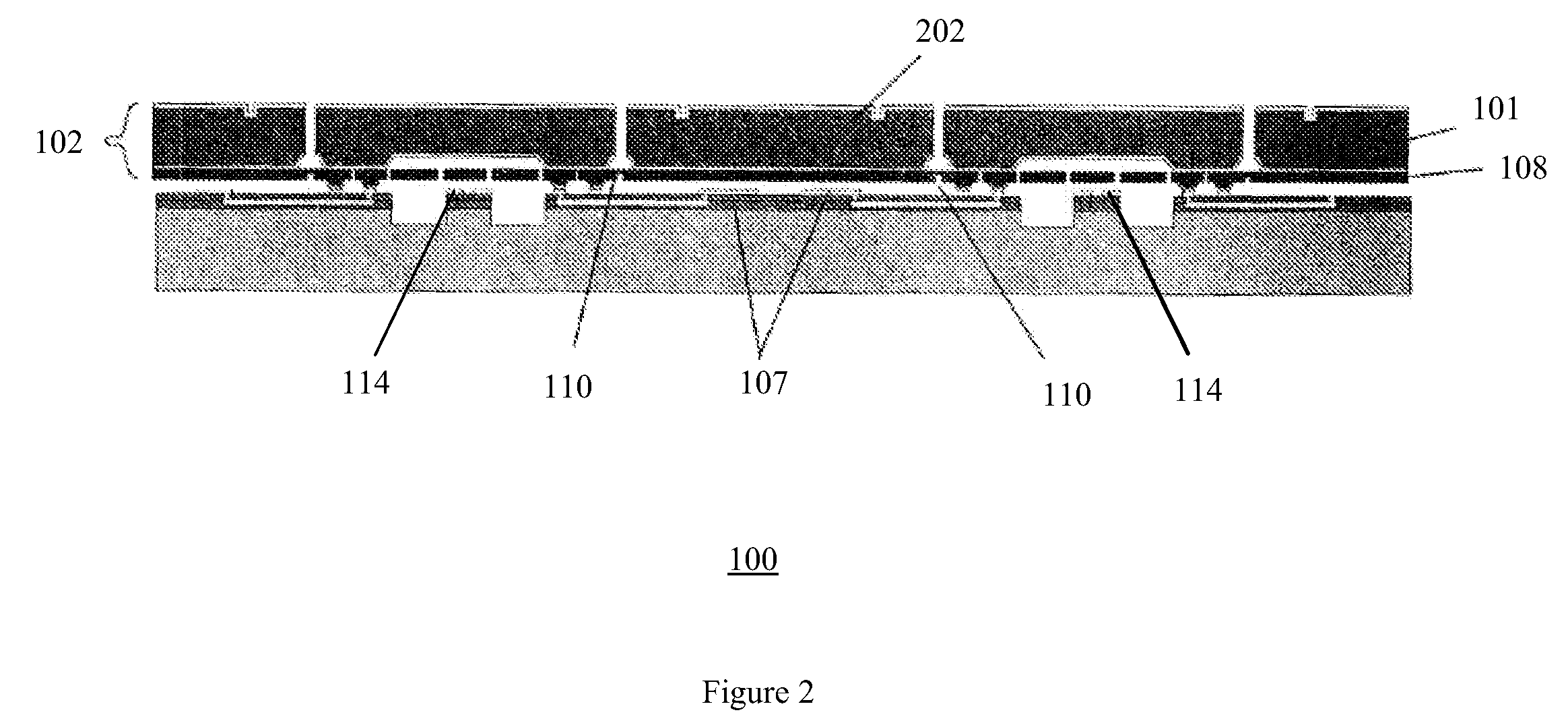
[0024]The following describes a preferred embodiment in accordance with the present invention. FIG. 1 is a MEMS device 100. The MEMS device 100 includes a MEMS cover structure 102 which comprises two bonded MEMS wafers 101 and 108 over a desired structure 114 on a substrate wafer 105. A plurality o...


PUM


Abstract

A MEMs (microelectromechanical systems) structure is provided. In one implementation, the MEMs structure includes a substrate wafer including a MEMs device formed on a surface of the substrate wafer, and a MEMs cover structure to cover the MEMs device formed on the surface of the substrate wafer. The MEMs cover structure comprises a first wafer bonded to a second wafer, in which only the first wafer of the MEMs cover structure is sawed through and not the second wafer of the MEMs cover structure during dicing of the MEMs structure.

Description

FIELD OF THE INVENTION[0001]The present invention relates generally to a MEMS structure and more specifically to a method and system for releasing such a structure after manufacturing.RELATED APPLICATIONS[0002]U.S. patent application Ser. No. 10 / 691,472, ENTITLED “Method of Making an X-Y Axis Dual-Mass Tuning Fork Gyroscope with Vertically Integrated Electronics and Wafer-Scale Hermetic Packaging,” filed Oct. 20, 2003.[0003]U.S. patent application Ser. No. 10 / 770,838, entitled “Vertically Integrated MEMS Structure,” filed Feb. 2, 2004.[0004]U.S. patent application Ser. No. 10 / 771,135, entitled “Vertical Integration of a MEMS Structure with Electronics in a Hermetically Sealed Cavity,” filed Feb. 2, 2004.BACKGROUND OF THE INVENTION[0005]MEMS technology has been under steady development for some time, and as a result various MEMS devices have been considered and demonstrated for several applications. MEMS technology is an attractive approach for providing many products, such as inerti...

Claims


Application Information

Patent Timeline
Patent Type & Authority Patents(United States)
IPC IPC(8): H01L21/46H01L21/326H01L21/78
CPCB81C1/00333
Inventor NASIRI, STEVEN S.FLANNERY, JR., ANTHONY FRANCISLIM, MARTIN
Owner INVENSENSE
Why Eureka
Try Eureka