

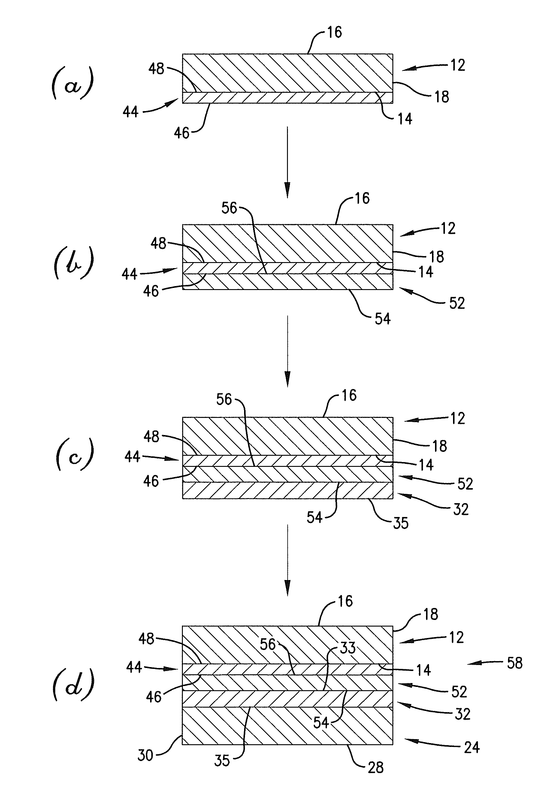
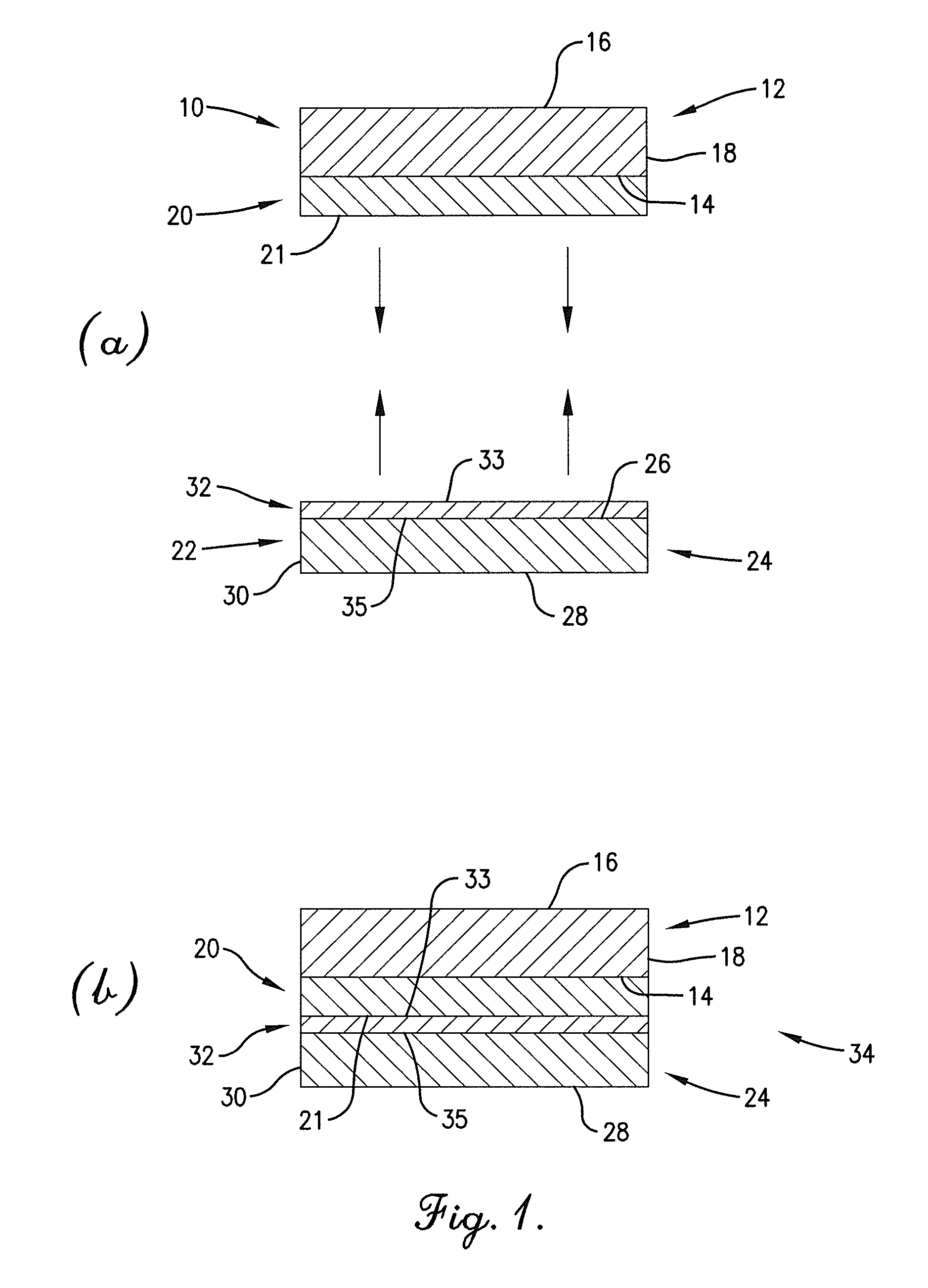
Multiple bonding layers for thin-wafer handling
a technology of multi-layer bonding and thin-wafer processing, applied in the field of multiple layers, can solve the problems of high thermal and mechanical stress on the device wafer, the inability to form backside electrical contacts that connect with the front-side circuitry, and the thinned device wafers that have been less than 100 microns thinned
- Summary
- Abstract
- Description
- Claims
- Application Information
AI Technical Summary
Benefits of technology
Problems solved by technology
Method used
Image

Examples
example 1
Composition of Cyclic Olefin Copolymer (COC) Bonding Composition A
[0114]In this formulation, 250 grams of an ethene-norbornene copolymer (APL 8008T, obtained from Mitsui Chemicals America, Inc., Rye Brook, N.Y.) and 3.125 grams of a phenolic antioxidant (IRGANOX 1010, obtained from BASF, Germany) were dissolved in 373.45 grams of R-limonene (obtained from Florida Chemical Co., Winter Haven, Fla.) and 373.45 grams of cyclooctane (obtained from Sigma-Aldrich, Inc., St. Louis, Mo.). The mixture was allowed to stir at room temperature until all of the components dissolved. The final solution had 25.31% solids.
example 2
Composition of COC Bonding Composition B
[0115]In this formulation, 210.31 grams of an ethane-norbornene copolymer (Topas 8007, obtained from Topas Advanced Polymers, Florence, Ky.) and 62.4 grams of a low-molecular-weight COC polymer (Topas TM, obtained from Topas Advanced Polymers, Florence, Ky.) were dissolved in 706 grams of R-limonene along with 4.0 grams of a phenolic antioxidant (Irganox 1010) and 14.5 grams of polyisobutylene (obtained from Scientific Polymer Products, Inc., Ontario, N.Y.) with a molecular weight of 2,800 Daltons. The mixture was allowed to stir at room temperature until all of ingredients were in solution. The solution had 29% solids.
example 3
Composition of COC Bonding Composition C
[0116]In this formulation, 50 grams of COC Bonding Composition B from Example 2 were mixed with 50 grams of R-limonene. The mixture was allowed to stir at room temperature to form a solution. The solution had 14.5% solids.
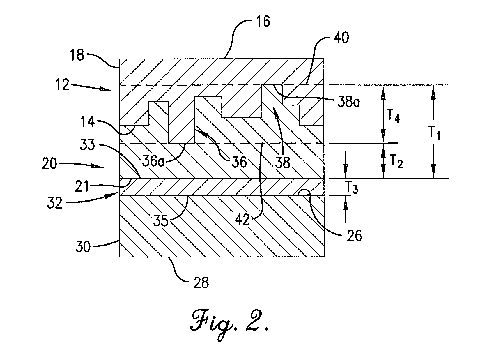
PUM
| Property | Measurement | Unit |
|---|---|---|
| softening temperature | aaaaa | aaaaa |
| thickness T1 | aaaaa | aaaaa |
| thickness T3 | aaaaa | aaaaa |
Abstract
Description
Claims
Application Information