Direct wafer bonded 2-D CUMT array

a technology of cumt array and wafer, applied in the field of direct wafer bonding to cumt array, can solve the problems of difficult wafer-to-wafer fusion bonding, inability to direct wire bond to array elements, and complex process of integrating through-wafer vias with cmuts

Active Publication Date: 2009-05-14
THE BOARD OF TRUSTEES OF THE LELAND STANFORD JUNIOR UNIV
View PDF7 Cites 130 Cited by
  • Summary
  • Abstract
  • Description
  • Claims
  • Application Information

AI Technical Summary

Problems solved by technology

These interconnects are necessary in situations where direct wire bonding to array elements is not feasible such as in fully populated 2D arrays; or due to space constraints, e.g., CMUTs for catheter-based applications.
Integrating through-wafer vias with CMUTs is a complex process requiring many lithographic steps.
After the deposition of the polysilicon, performing wafer-to-wafer fusion bonding is difficult.
The complex through-wafer interconnect fabrication steps degrade wafer surface smoothness; therefore, an expensive chemical-mechanical polishing step is required to get bondable surface quality in terms of roughness.
Furthermore, these steps add stress to the wafer, which results in a reduced radius of curvature.
To date, no successful through-wafer via fabrication technique has been demonstrated that is compatible with the wafer-bonding technique of making CMUTs.
This particular requirement presents drawbacks in the fabrication process.
However, it is then a challenge to separate the carrier wafer and the membrane after the flip-chip bonding.
The adhesive material can swell in the solvent and, therefore, create stress that can break the CMUT membranes.
Further, the CMUT cell is unprotected during the fabrication process, resulting in contamination of the cell cavity.
The resultant CMUT cells have limited design flexibility and suffer from reliability degradation due to electrical breakdown.

Method used


Image

  • Direct wafer bonded 2-D CUMT array
  • Direct wafer bonded 2-D CUMT array
  • Direct wafer bonded 2-D CUMT array

Examples


Embodiment Construction

[0082]Although the following detailed description contains many specifics for the purposes of illustration, anyone of ordinary skill in the art will readily appreciate that many variations and alterations to the following exemplary details are within the scope of the invention. Accordingly, the following preferred embodiment of the invention is set forth without any loss of generality to, and without imposing limitations upon, the claimed invention.

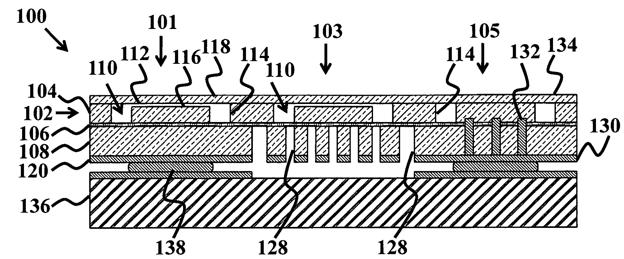
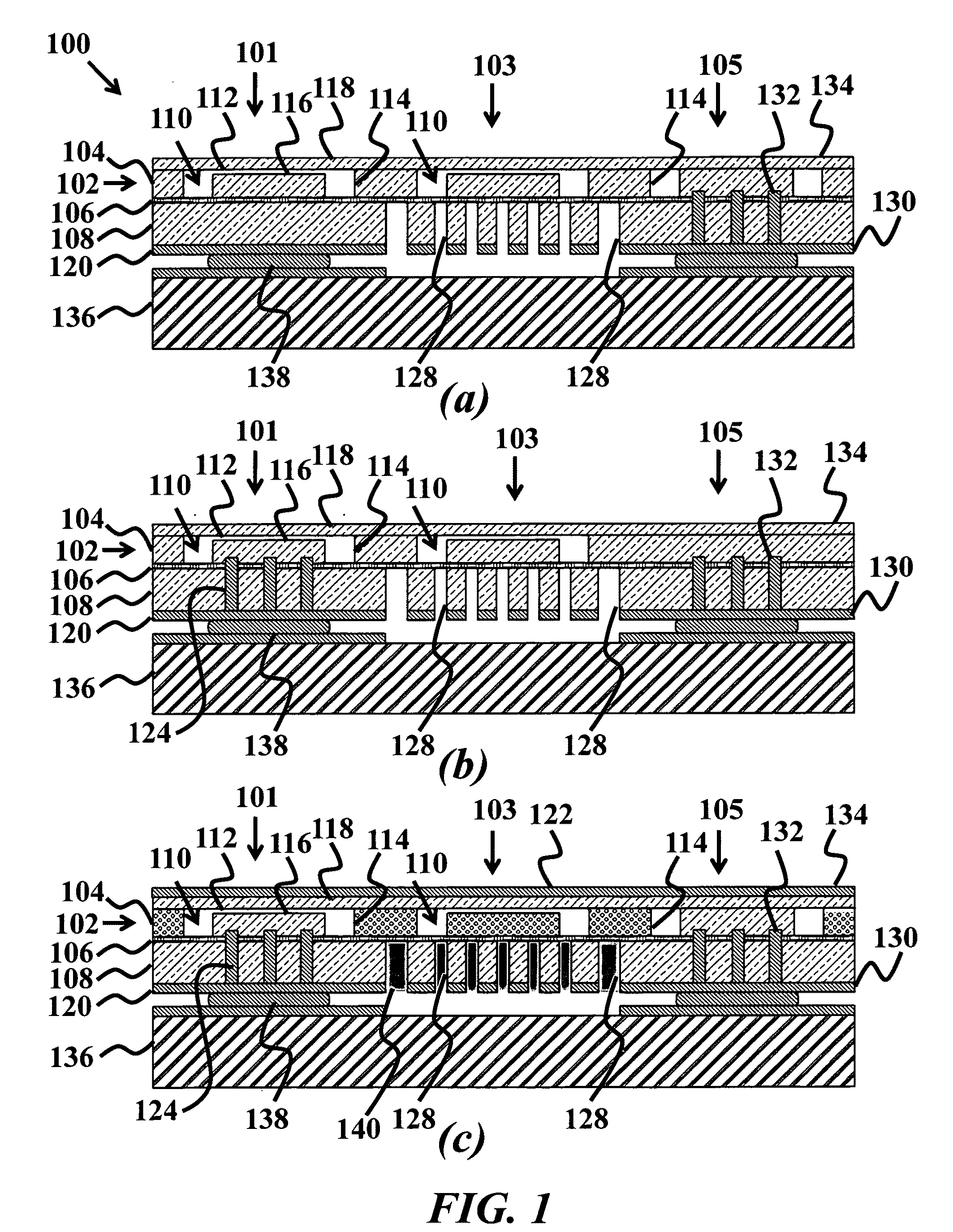
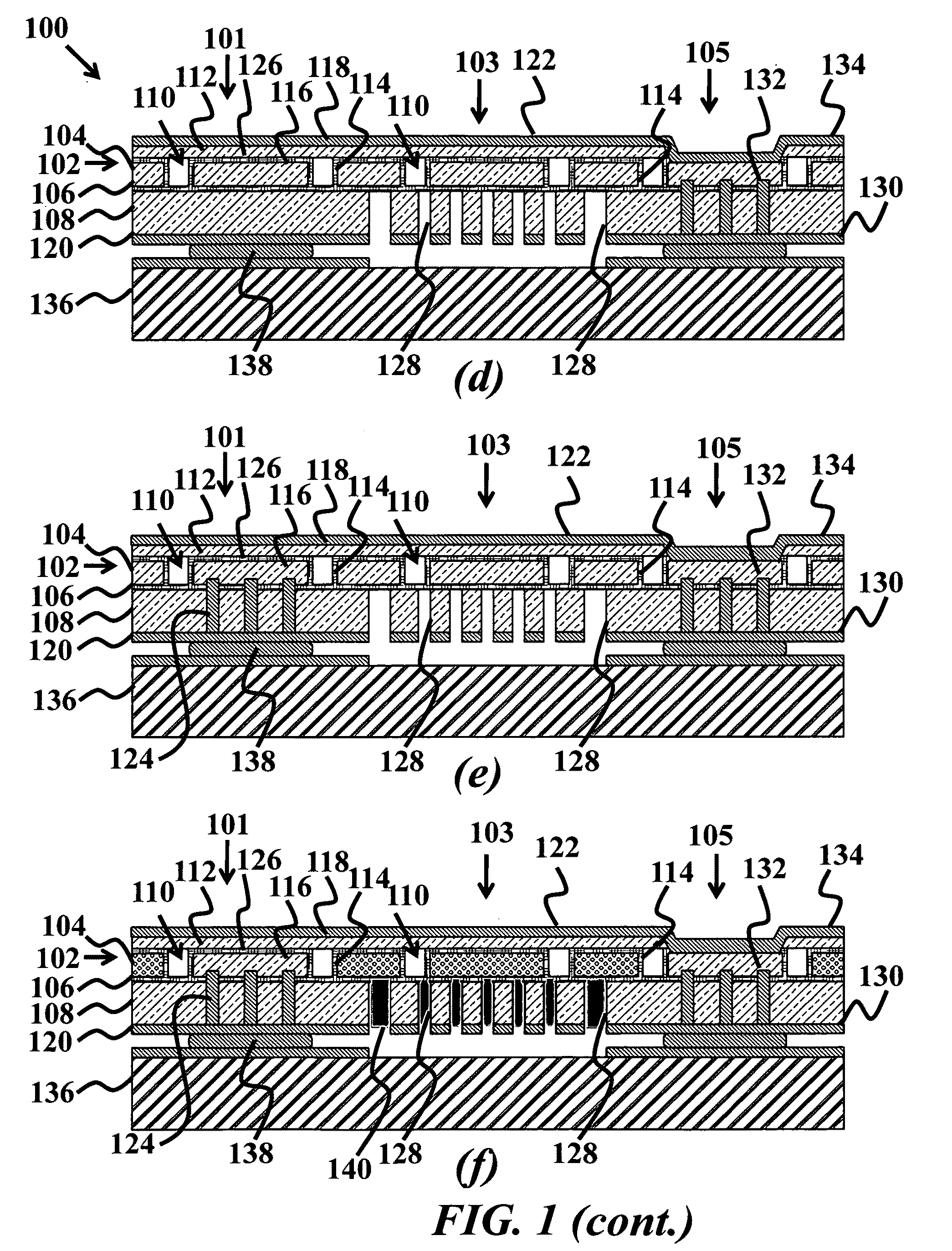
[0083]The invention includes a device and method for providing fully populated two dimensional (2D) capacitive micromachined ultrasonic transducer arrays, based on direct wafer bonding. The advantages are: (1) a reduced number of fabrications steps; (2) an improved CMUT cell structure (increased electrical breakdown voltage and reduced parasitic capacitance, (3) a better design flexibility and a high controllability for the whole frequency range in which CMUT arrays can be used (1 kHz-300 MHz); (4) a built-in support structure that elimin...


PUM

PropertyMeasurementUnit
thicknessaaaaaaaaaa
hole diameteraaaaaaaaaa
thicknessaaaaaaaaaa

Abstract

A capacitive micromachined ultrasonic transducer (CMUT) array connected to a separate electronic unit is provided. The CMUT array includes at least two active elements, a ground element at the array end, and a non-active element having isolation trenches disposed between the active and ground elements. The active element includes a doped first silicon layer, a doped second silicon layer, and a first insulating layer disposed there between. A cavity is in the first silicon layer having a cross section that includes vertical portions disposed at each end of a horizontal portion, and the vertical portion spans from the first insulating layer through the first silicon layer such that a portion of the first silicon layer is isolated by the first insulating layer and the cavity. A membrane layer on the first silicon layer spans the cavity. A bottom electrode is disposed on the bottom of the second silicon layer.

Description

CROSS-REFERENCE TO RELATED APPLICATIONS[0001]This application is cross-referenced to and claims the benefit from U.S. Provisional Patent Application 60 / 999,641 filed Oct. 18, 2007, which is hereby incorporated by reference.FIELD OF THE INVENTION[0002]The invention relates generally to electrostatic transducers. More particularly, the invention relates to electrostatic transducer arrays and their fabrication.BACKGROUND[0003]Capacitive micromachined ultrasonic transducers (CMUT) have gained much attention as an ultrasound transducer technology to complement / replace piezoelectric transducers. CMUTs have been shown to enhance existing medical ultrasound imaging probes, and new applications inappropriate for piezoelectrics have been explored using CMUTs. In medical imaging, examples include annular ring-shaped arrays, micro-linear arrays, fully populated 2D arrays, flexible arrays, and 2D reconfigurable arrays. In medical therapy, CMUTs can provide MR-compatible high-intensity focused ul...

Claims


Application Information

Patent Timeline
Patent Type & Authority Applications(United States)
IPC IPC(8): H04R19/00H02N11/00H04R31/00
CPCB06B1/0292Y10T29/49005H02N1/008
Inventor KUPNIK, MARIOKHURI-YAKUB, BUTRUS T.
Owner THE BOARD OF TRUSTEES OF THE LELAND STANFORD JUNIOR UNIV
Why Eureka
Try Eureka