High efficiency multi-active layer tunnel regenerated white light emitting diode

a multi-active layer tunnel and white light-emitting diode technology, applied in the field of optoelectronics, can solve the problems of not being competitive with standard white-light sources in either performance or cost, and achieve the effects of improving the current spreading of led, improving the current spreading, and increasing the luminance of each light cell

Inactive Publication Date: 2005-03-31
BEIJING UNIV OF TECH
View PDF5 Cites 141 Cited by
  • Summary
  • Abstract
  • Description
  • Claims
  • Application Information

AI Technical Summary

Benefits of technology

[0020] 2. The tunnel junction improves the current spreading of LED, so the more the tunnel junction, the better the current spreading. There needn't the thickness current spreading layer due to the thin tunnel junction.
[0021] 3. The each light cell of the invention can be multiple active-layer which emit the same wavelength of light, so the luminance of each light cell can be increased importantly, thus the efficiency and

Problems solved by technology

White-light LED lamps are commercially available, but they are not comp

Method used


Image

  • High efficiency multi-active layer tunnel regenerated white light emitting diode
  • High efficiency multi-active layer tunnel regenerated white light emitting diode
  • High efficiency multi-active layer tunnel regenerated white light emitting diode

Examples


Embodiment Construction

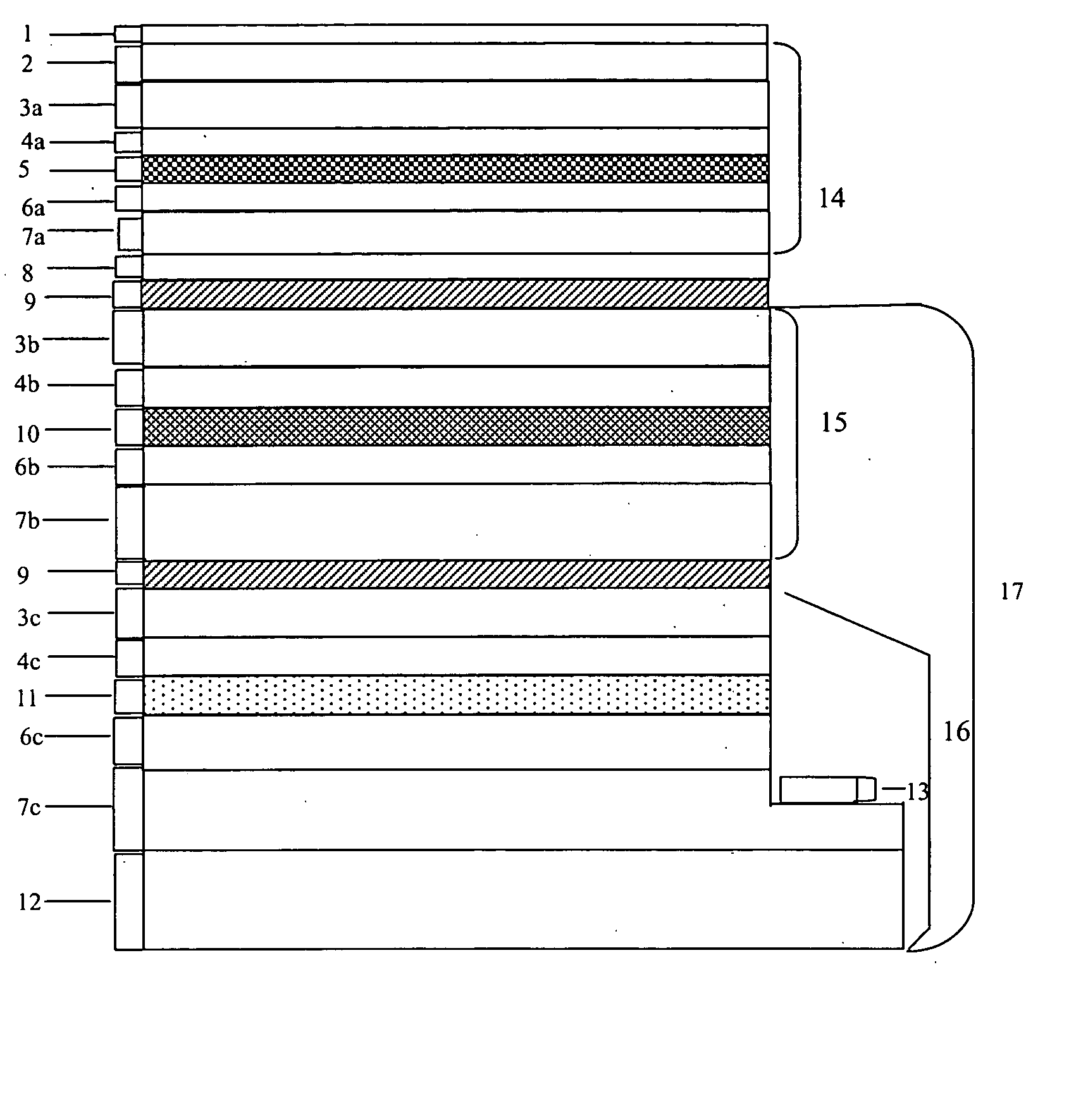
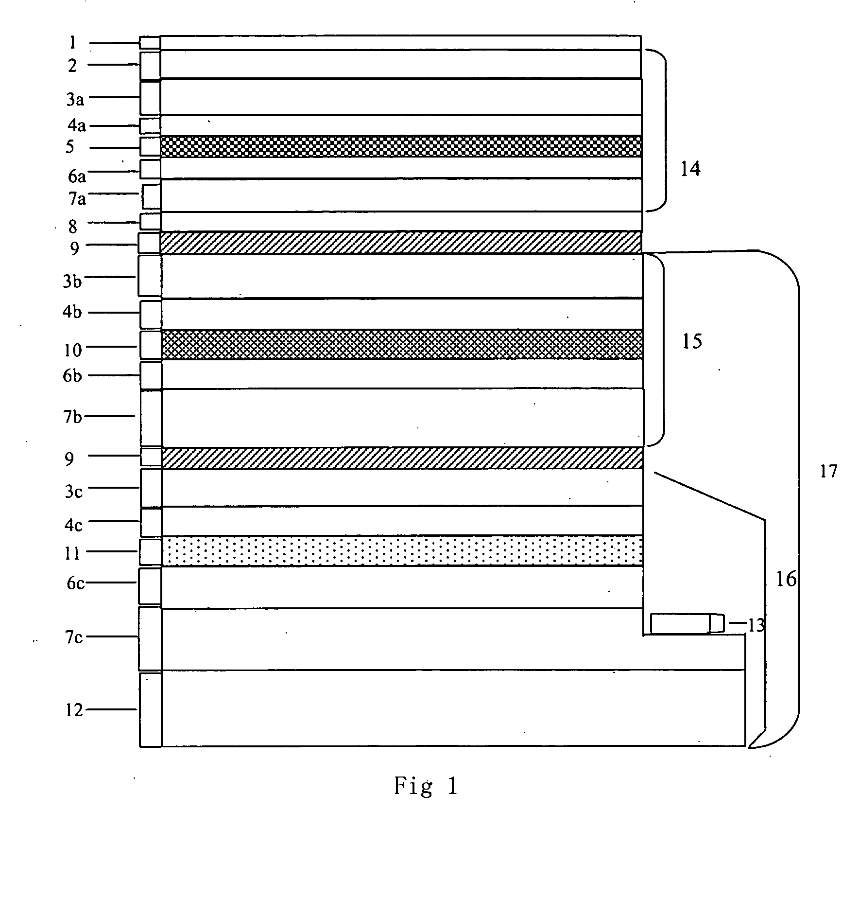
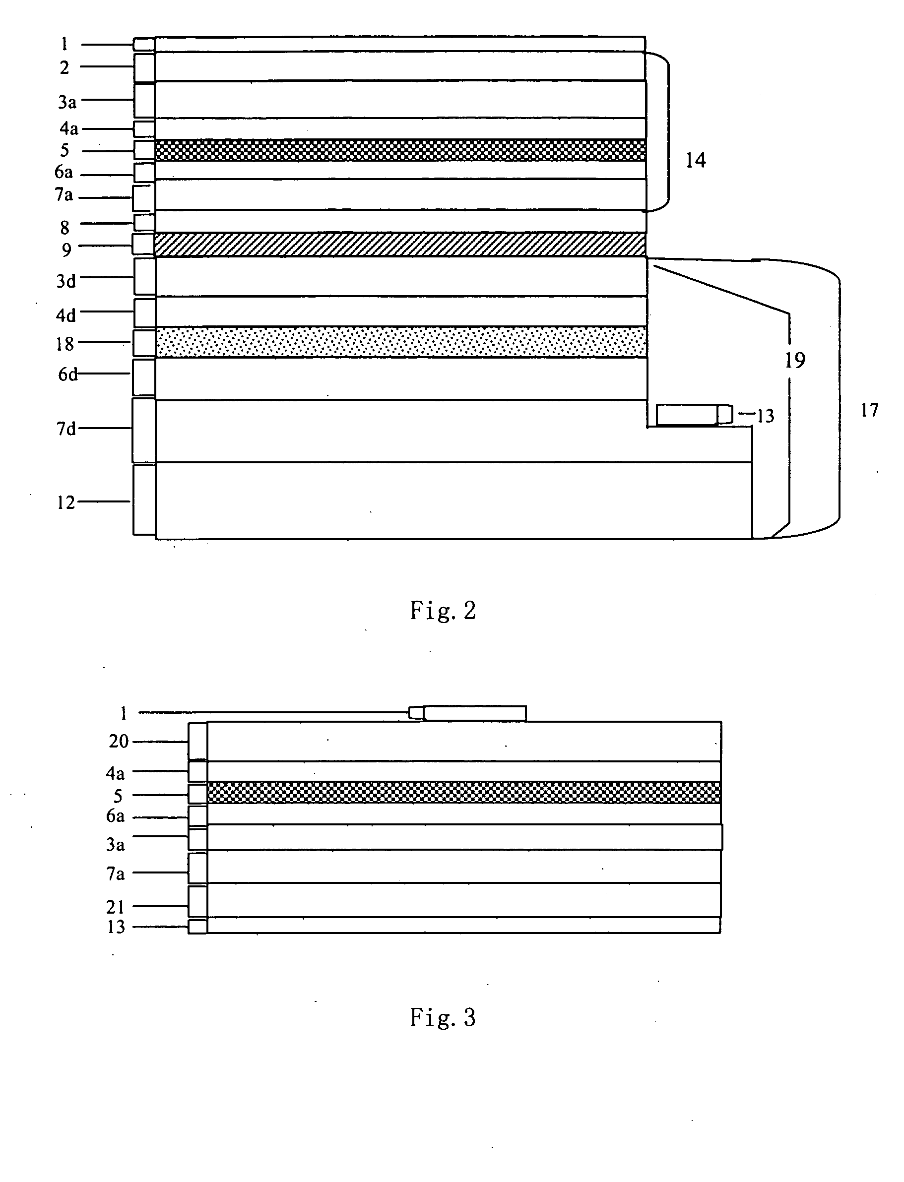
[0032] As an example of the tunnel regenerated white LED is schematically shown as FIG. 7, the fabrication process as following: [0033] 1. The red light cell was grown in metal-organic chemical vapor deposition (MOCVD) layer by layer: after growing a buffer layer of n+GaAs, then N++ / P++ GaAs tunnel junction 9, N-GalnP buffer layer 7a, N-AllnP down confinement layer 6a, AlGaInP / GaInP hetero junction active layer 5, p-AllnP up confinement layer 4a, P++ GaAs cap layer 2. And then thermal deposit or sputter p type metal electrode Ti / Au 1 on the top of p cap layer. And then grinding or liftoff the GaAs substrate and get the red light cell.

[0034] 2. The green and blue light cell are grown in metal-organic chemical vapor deposition (MOCVD) layer by layer: After growing a n type buffer 7c on the top of sapphire or SiC substrate, n type InGaN down confinement layer 6c, InGaN / GaN multi-quantum wells blue active layer 11, p-AlGaN up confinement layer 4c, AlInN / GaN DBR blue light reflector lay...


PUM


Abstract

A high efficiency and high brightness multi-active layer tunneling regenerated white color semiconductor light emitting diode having a p type electrode 1, a monolithic red light cell 14, a tunnel junction 9, a monolithic green light 15 and blue light cell 16 (or a monolithic cyan light cell 19), wherein each of said cells are electrically connected by tunnel junctions 9, and the red cell physically connected with blue and green cell (or cyan cell) by wafer bonding layer 8. The lights from each cell synthesize white color light. The white light emitting diode only has one time optical-electrical conversion, so the quantum efficiency is high. Moreover, the white LED totally made from semiconductor materials, the lifetime of the white LED lamp is not limited by the relatively short lifetime of fluorescent material.

Description

FIELD OF THE INVENTION [0001] The present invention relates to the structure of a high efficiency multi-active layer tunnel regenerated white light emitting diode and the method of manufacturing the same, which belong to the field of optoelectronics. BACKGROUND OF THE INVENTION [0002] The design structure and problem of conventional white LED: [0003] 1. one kind of conventional white LED normally based on the mixing of red, green and blue pure monochromatic light LED which named pixel white LED shown as FIG. 3, 4 and 5. However, it has long been a disadvantage of above white light-emitting diodes: for the pixel white LED, not all colors of visible light were available with the same luminous intensity. The efficiency of light-emitting diodes decreases as the wavelength decreases, that is from red, via green, to blue. The brightness of red and green light-emitting diodes was very good. And such a white light-emitting device is costly. Further, the design of the drive system is very co...

Claims


Application Information

Patent Timeline
IPC IPC(8): H01L29/08H01L33/00H01L33/08
CPCH01L33/08H01L33/0016
Inventor SHEN, GUANGDIGUO, XIAGUO, WEILINGGAO, GUO
Owner BEIJING UNIV OF TECH
Why Eureka
Try Eureka