Supercharge Your Innovation With Domain-Expert AI Agents!

Pixel unit, manufacturing method thereof and imaging device

A technology of pixel units and doped regions, applied in radiation control devices, electrical components, electrical solid devices, etc., can solve problems such as unsatisfactory performance, and achieve the effects of improving quantum effects, reducing leakage, and reducing light absorption distance

Active Publication Date: 2018-05-18
淮安西德工业设计有限公司
View PDF5 Cites 4 Cited by
  • Summary
  • Abstract
  • Description
  • Claims
  • Application Information

AI Technical Summary

Problems solved by technology

However, in the case of using amorphous silicon to form devices such as pass transistors, the performance may not be ideal
Therefore, there are many difficult challenges in forming pixels from amorphous silicon

Method used

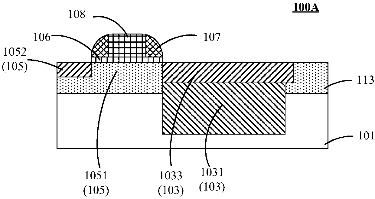
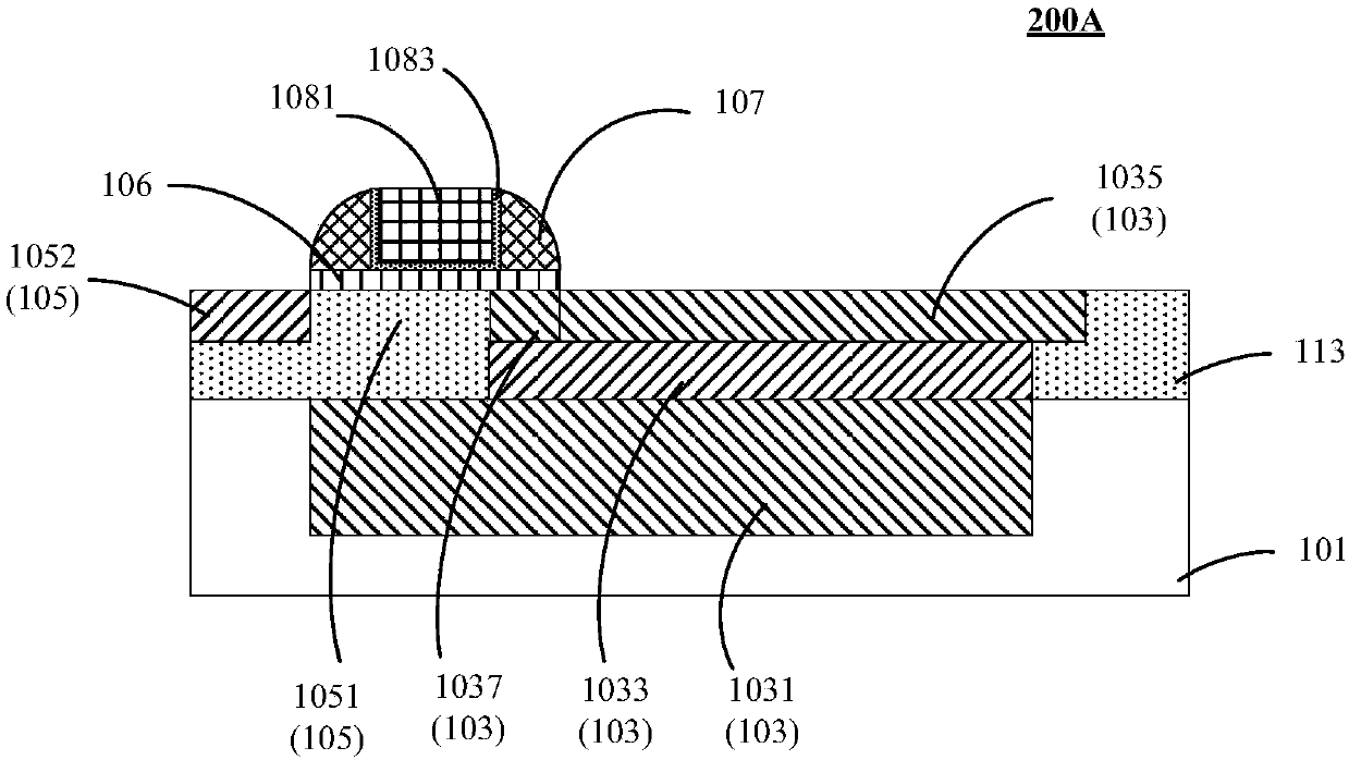
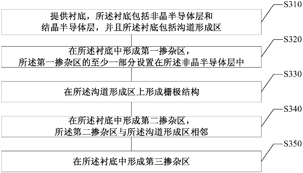

Image

  • Pixel unit, manufacturing method thereof and imaging device
  • Pixel unit, manufacturing method thereof and imaging device
  • Pixel unit, manufacturing method thereof and imaging device

Examples


Embodiment Construction

[0033] Various exemplary embodiments of the present disclosure will now be described in detail with reference to the accompanying drawings. It should be noted that the relative arrangements of components and steps, numerical expressions and numerical values ​​set forth in these embodiments do not limit the scope of the present disclosure unless specifically stated otherwise. In addition, techniques, methods, and devices known to those of ordinary skill in the relevant art may not be discussed in detail, but under appropriate circumstances, the techniques, methods, and devices should be considered as part of the authorized description.

[0034] In the specification and claims, the words "front", "rear", "top", "bottom", "above", "under", etc., if present, are used for descriptive purposes and not necessarily to describe a constant relative position. It is to be understood that the terms so used are interchangeable under appropriate circumstances such that the embodiments of th...


PUM


Abstract

The invention discloses and relates to a pixel unit, a manufacturing method thereof and an imaging device. The pixel unit can comprises a substrate, wherein the substrate comprises an amorphous semiconductor layer and a crystal semiconductor layer on the amorphous semiconductor layer, the substrate comprises a first part and a second part, the first part is used for a photoelectric device, the second part is used for coupling with the photoelectric device, the first part comprises a first doping region and a second doping region on the first doping region, the conductive type of the second doping region is same as the conductive type of the first doping region, the second part comprises a channel formation region adjacent to the second doping region, the conductive type of the channel formation region is opposite to the conductive type of the second doping region, at least one part of the first doping region is arranged in the amorphous semiconductor layer, and at least one part of thesecond doping region is arranged in the crystal semiconductor layer.

Description

technical field [0001] The present disclosure relates to a pixel unit, a method of manufacturing the same, and an imaging device. Background technique [0002] Image sensors can be used to sense radiation (eg, optical radiation, including but not limited to visible light, infrared rays, ultraviolet rays, etc.) to generate corresponding electronic signals. It is widely used in digital cameras and other electro-optical devices. [0003] Compared with crystalline silicon (c-Si), amorphous silicon (α-Si) has relatively high light absorption efficiency, especially for the visible light range, and has low leakage. However, in the case of forming devices such as pass transistors using amorphous silicon, the performance may not be ideal. Therefore, there are many difficult challenges in forming pixels using amorphous silicon. [0004] Therefore, it is necessary to propose a new technology to solve one or more problems or challenges in the above-mentioned prior art. Contents of ...

Claims


Application Information

Patent Timeline
Patent Type & Authority Applications(China)
IPC IPC(8): H01L27/146
CPCH01L27/14601H01L27/14683
Inventor 柯天麒姜鹏汤茂亮
Owner 淮安西德工业设计有限公司
Features
  • R&D
  • Intellectual Property
  • Life Sciences
  • Materials
  • Tech Scout
  • Unparalleled Data Quality
  • Higher Quality Content
  • 60% Fewer Hallucinations
Learn More