An array substrate, its preparation method, and a display device

An array substrate and substrate substrate technology, which is applied in the manufacture of semiconductor/solid-state devices, semiconductor devices, electrical components, etc., can solve the problems of display life, display effect and other adverse performance effects, film layer morphology (non-uniform thickness, etc.) Achieve the effect of optimizing the drying process and improving the uniformity of film formation

Active Publication Date: 2020-12-25
BOE TECH GRP CO LTD
View PDF4 Cites 0 Cited by
  • Summary
  • Abstract
  • Description
  • Claims
  • Application Information

AI Technical Summary

Problems solved by technology

[0004] However, since the light-emitting area of ​​the sub-pixel is rectangular, in this way, when the ink printed on the light-emitting area of ​​the corresponding sub-pixel in the pixel definition layer is dried under the same drying process, the ink located in the light-emitting area of ​​the sub-pixel is along the long side. There is a large difference in the surface tension distribution and migration distance in the short-side direction, which makes the morphology (thickness) of the film layer formed after drying uneven, which in turn leads to adverse effects on the lifespan and display effect of the display.

Method used


Image

  • An array substrate, its preparation method, and a display device
  • An array substrate, its preparation method, and a display device
  • An array substrate, its preparation method, and a display device

Examples


Embodiment Construction

[0033] The following will clearly and completely describe the technical solutions in the embodiments of the present invention with reference to the accompanying drawings in the embodiments of the present invention. Obviously, the described embodiments are only some, not all, embodiments of the present invention. Based on the embodiments of the present invention, all other embodiments obtained by persons of ordinary skill in the art without making creative efforts belong to the protection scope of the present invention.

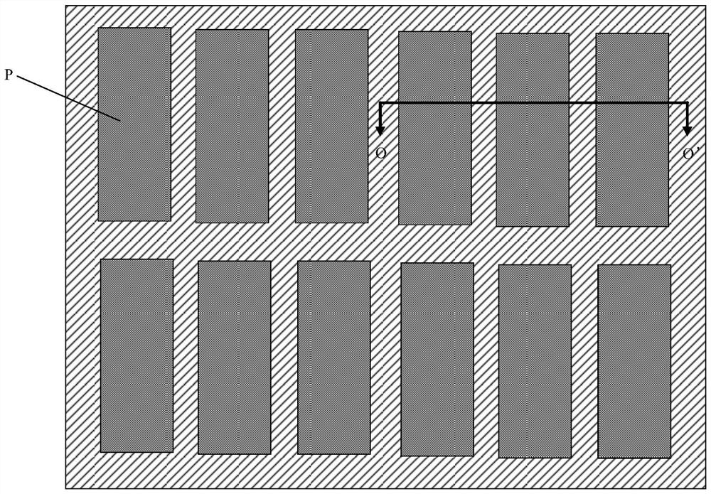
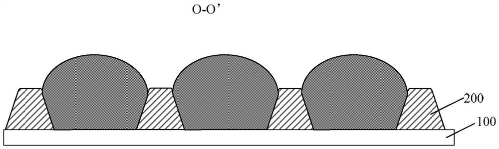
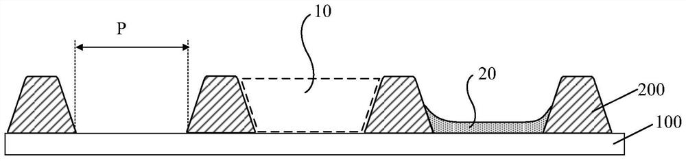
[0034] An embodiment of the present invention provides an array substrate, the array substrate includes a pixel definition layer (Pixel Define Layer, PDL) 200 disposed on the base substrate 100 for defining the sub-pixel light-emitting area P, of course, the pixel definition layer can also be It is called a pixel definition layer; the pixel definition layer 200 is a hollow 10 (also called an opening) at the position of the sub-pixel light-emitting area P, and a...


PUM

PropertyMeasurementUnit
thicknessaaaaaaaaaa

Abstract

Embodiments of the present invention provide an array substrate, a preparation method, and a display device, which relate to the field of display technology and can improve the uniformity of a light-emitting functional layer. The array substrate includes a pixel definition layer arranged on the base substrate to define the sub-pixel light-emitting area, the pixel-definition layer is hollowed out at the position of the sub-pixel light-emitting area, and a light-emitting functional layer is arranged in the hollow; the pixel definition layer is located at the position of the sub-pixel light-emitting area Cutout sides feature raised features.

Description

technical field [0001] The present invention relates to the field of display technology, in particular to an array substrate, a preparation method, and a display device. Background technique [0002] Organic Light Emitting Diode (OLED) displays have been widely used in computers, mobile phones, etc. Various electronic devices including electronic products. [0003] Such as Figure 1a and Figure 1b ( Figure 1a As shown in the schematic cross-sectional view along the 0-O' position), in the prior art, the OLED display is generally produced by printing ink to the pixels on the base substrate 100 provided with the pixel definition layer 200 by inkjet printing. In the light-emitting region P corresponding to the sub-pixel in the definition layer 200 , excess solvent is removed through subsequent processes such as drying to form an organic light-emitting functional layer. [0004] However, since the light-emitting area of ​​the sub-pixel is rectangular, in this way, when the i...

Claims


Application Information

Patent Timeline
Patent Type & Authority Patents(China)
IPC IPC(8): H01L27/32H01L51/56
CPCH10K59/122H10K71/135H10K59/353H10K59/173H10K50/11H10K71/191
Inventor 代青
Owner BOE TECH GRP CO LTD
Why Eureka
Try Eureka