Liquid crystal display panel processing method

A technology of liquid crystal display panels and processing methods, applied in nonlinear optics, instruments, optics, etc., can solve problems such as deterioration of panel pits, and achieve the effects of avoiding excessive corrosion, improving display quality, and avoiding uneven panel display

Active Publication Date: 2018-05-25
WUHAN CHINA STAR OPTOELECTRONICS TECH CO LTD
View PDF5 Cites 2 Cited by
  • Summary
  • Abstract
  • Description
  • Claims
  • Application Information

AI Technical Summary

Problems solved by technology

[0005] In view of this, the present invention provides a method for processing liquid crystal display panels, which is used to solve the problem in the prior art that the thinning process of the panel will deteriorate the pits on the panel

Method used


Image

  • Liquid crystal display panel processing method
  • Liquid crystal display panel processing method
  • Liquid crystal display panel processing method

Examples


Embodiment Construction

[0037] The technical solutions in the embodiments of the present invention are clearly and completely described below in conjunction with the accompanying drawings and embodiments. Obviously, the described embodiments are only part of the embodiments of the present invention, not all of them. It should be pointed out that the specific embodiments described here are only used to explain the present invention, not to limit the present invention.

[0038] In view of the fact that the thinning process of the panel in the prior art will deteriorate the pits on the panel, the embodiment of the present invention firstly provides a processing method for a liquid crystal display panel, including the following steps:

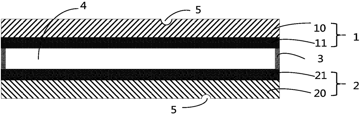
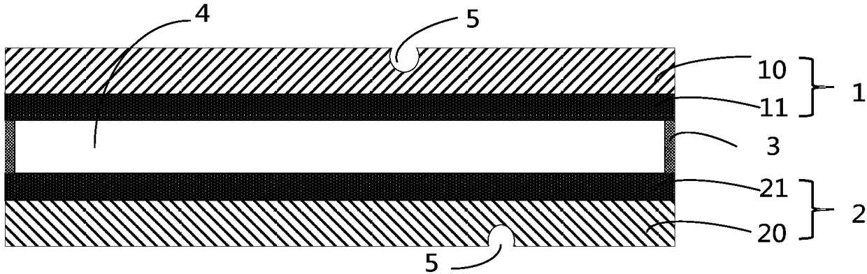
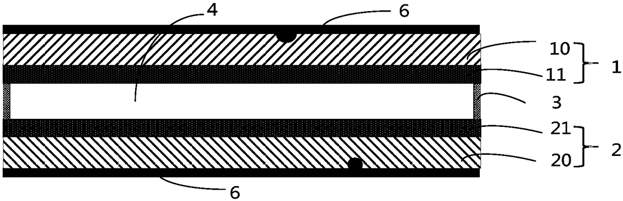
[0039]Provide a boxed liquid crystal display panel as shown in Figure 1, the boxed liquid crystal display panel includes a thin film transistor (TFT) array substrate 1 and a color filter (Color Filter, CF) substrate 2 arranged oppositely, and a clip The frame glue 3 and t...


PUM

PropertyMeasurementUnit
thicknessaaaaaaaaaa
wavelengthaaaaaaaaaa

Abstract

The invention provides a liquid crystal display panel processing method. The method comprises the steps that a liquid display panel is provided, the liquid display panel comprises a thin film transistor array substrate, a color film substrate and a liquid crystal layer clamped between the thin film transistor array substrate and the color film substrate, and pits exist on surfaces, facing away from the liquid crystal layer, of the thin film transistor array substrate and the color film substrate; an organic silicon resin film layer or a silicon oxide film layer is formed respectively on the surfaces, facing away from the liquid crystal layer, of the thin film transistor array substrate and the color film substrate to fill the existed pits on the two substrates of the liquid crystal displaypanel to obtain a flattened liquid crystal display panel; thinning treatment is conducted on the flattened liquid crystal display panel. The existence of the organic silicon resin film layer or the silicon oxide film layer can fill the pits which might exist on the panel, and probability that the pits are deteriorated when the thinning treatment is conducted on the panel is reduced to improve display quality of the panel.

Description

technical field [0001] The invention relates to the technical field of liquid crystal display panels, in particular to a processing method for a liquid crystal display panel. Background technique [0002] In recent years, liquid crystal display (Liquid Crystal Display, LCD) technology has been rapidly popularized due to its unique advantages of low power consumption, low radiation, light weight and convenience. Among them, the thin film transistor liquid crystal display (Thin Film Transistor-Liquid Crystal Display, TFT-LCD) uses thin film transistors (Thin Film Transistor, TFT) to generate voltage to control the direction of liquid crystal molecules to achieve screen display, TFT-LCD panel with its The advantages of fast response speed and large viewing angle have been widely used in electronic devices such as mobile phones. [0003] A TFT-LCD panel usually includes a TFT array substrate and a color filter substrate arranged opposite to each other, and a liquid crystal laye...

Claims


Application Information

Patent Timeline
Patent Type & Authority Applications(China)
IPC IPC(8): G02F1/13
CPCG02F1/1303G02F1/1309
Inventor 李成
Owner WUHAN CHINA STAR OPTOELECTRONICS TECH CO LTD
Why Eureka
Try Eureka