Server architecture and running method
An operation method and server technology, applied in the field of servers, can solve the problems of unfavorable high integration of modules, inability to save BIOS storage chips in server architecture, high hardware cost, etc., and achieve the advantages of high integration, enhanced intelligence, and reduced hardware costs Effect
- Summary
- Abstract
- Description
- Claims
- Application Information
AI Technical Summary
Problems solved by technology
Method used
Image
Examples
Embodiment 1
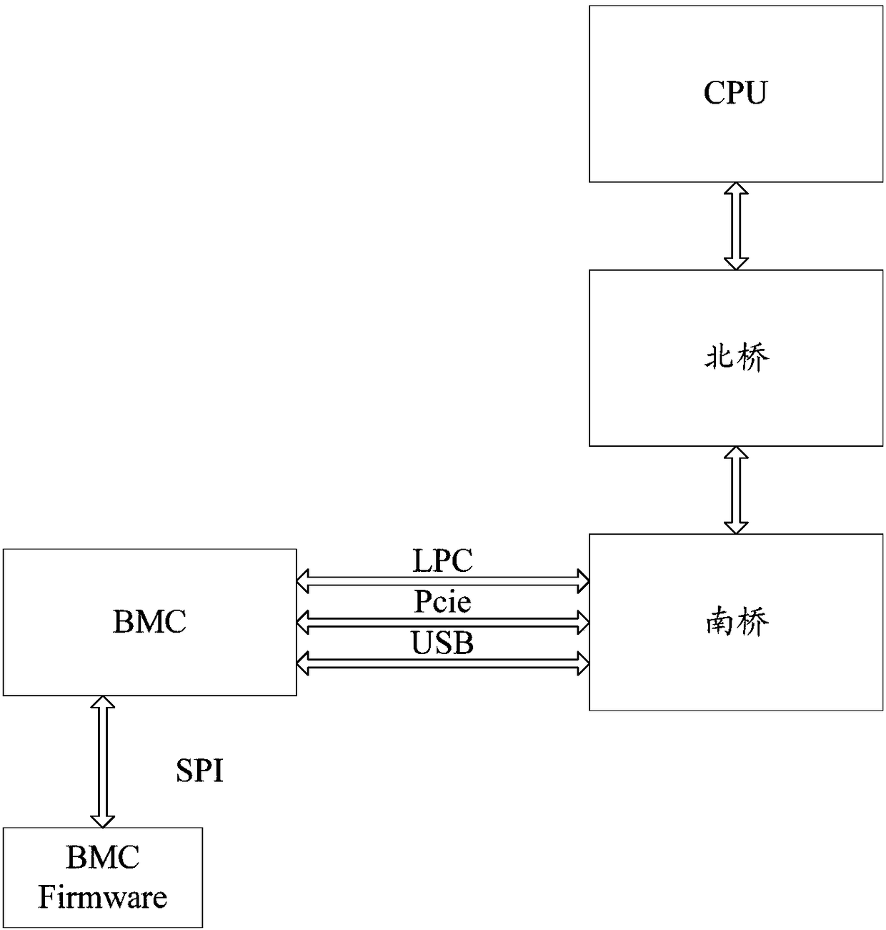
[0031] figure 1 It is a structural block diagram of the server architecture provided by the embodiment of the present invention, and is described in detail as follows:
[0032] A server architecture, including processor CPU, north bridge chip, south bridge chip, described server architecture also includes baseboard management controller BMC;
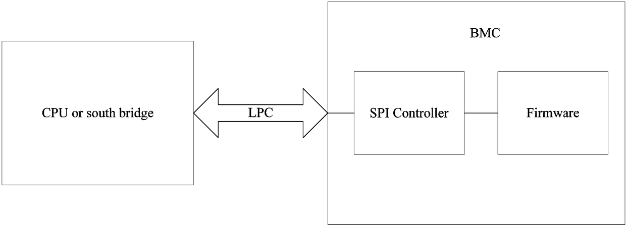
[0033] The CPU or the south bridge chip is connected with the SPI controller serial peripheral bus controller of the BMC through the LPC low pin number interface;
[0034] The storage medium of the BMC is divided into two areas, the first area stores the BMC code, and the second area stores the BIOS code.
[0035] figure 2 The connection diagram of the CPU or the south bridge chip and the BMC provided for the embodiment of the present invention is described in detail as follows:
[0036] Wherein, the south bridge chip is connected to the BMC through the LPC low pin number interface, the Pcie interface and the USB interface.
[0037]...
Embodiment 2
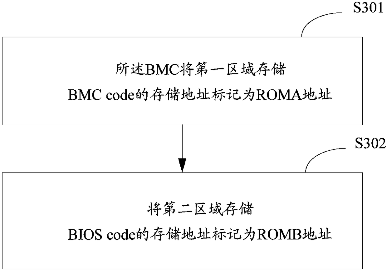
[0044] image 3 It is the implementation flowchart of the operating method provided by the embodiment of the present invention, and is described in detail as follows:
[0045] S301, the BMC marks the storage address of the BMC code stored in the first area as a ROMA address;
[0046] S302. Mark the storage address where the BIOS code is stored in the second area as a ROMB address;
[0047] Wherein, the ROMB address and the ROMA address are different addresses.
[0048] Figure 4 A sample diagram of dividing the ROMA address and the ROMB address of the BMC Flash ROM provided by the embodiment of the present invention.
[0049] The CPU or south bridge is connected to the SPI controller of the BMC through the LPC, and the firmware of the BMC is hung under the SPI controller.
[0050] In the Rom map, the storage address where the Firmware stores the BMC code is marked as a ROMA address, and the storage address where the Firmware stores the BIOS code is marked as a ROMA address...
Embodiment 3
[0053] Figure 5 It is an effect diagram of dividing the ROMA address and the ROMB address of the BMC Flash ROM provided by the embodiment of the present invention, and is described in detail as follows:
[0054] exist Figure 5 Among them, the 32MB BMC rom is divided into two areas, 0-24MB is the first area for storing BMCcode, and 24MB to 32MB is the second area for storing BIOS code area.
[0055] The setup process is as follows:
[0056] 1) Set up on the SPI controller of the BMC,
[0057] Divide the 32MB Flash Rom into two areas, ROMA: 00000000h~18000000h (24MB) and ROMB: 18000000h~1f000000h (8MB).
[0058] 2) According to AST2400 design instructions:
[0059] Control SCU2C: Misc.Control Register offset 2C position, Bit0, set to Enable.
[0060] The BMC code is placed at 00000000h~18000000h, and the execution of the BMC code remains unchanged. The BIOS code is placed between 18000000h and 1f000000h.
[0061] When the CPU accesses the SPI controller through LPC, the...
PUM
 Abstract
Description
Claims
Application Information


