Supercharge Your Innovation With Domain-Expert AI Agents!

Semiconductor device with metallization structure on opposite sides of a semiconductor portion

A metallized structure, semiconductor technology, applied in the fields of semiconductor/solid-state device parts, semiconductor devices, semiconductor/solid-state device manufacturing, etc., can solve the problems of complex operation, complex operation and cutting of thin semiconductor die

Active Publication Date: 2018-05-25
INFINEON TECH AG
View PDF7 Cites 0 Cited by
  • Summary
  • Abstract
  • Description
  • Claims
  • Application Information

AI Technical Summary

Problems solved by technology

As the thickness of semiconductor die decreases, the processing of semiconductor substrates to obtain thin semiconductor die becomes more complex in terms of handling and dicing
Additionally, the manipulation of separated thin semiconductor dies becomes more complex

Method used


Image

  • Semiconductor device with metallization structure on opposite sides of a semiconductor portion
  • Semiconductor device with metallization structure on opposite sides of a semiconductor portion
  • Semiconductor device with metallization structure on opposite sides of a semiconductor portion

Examples


Embodiment Construction

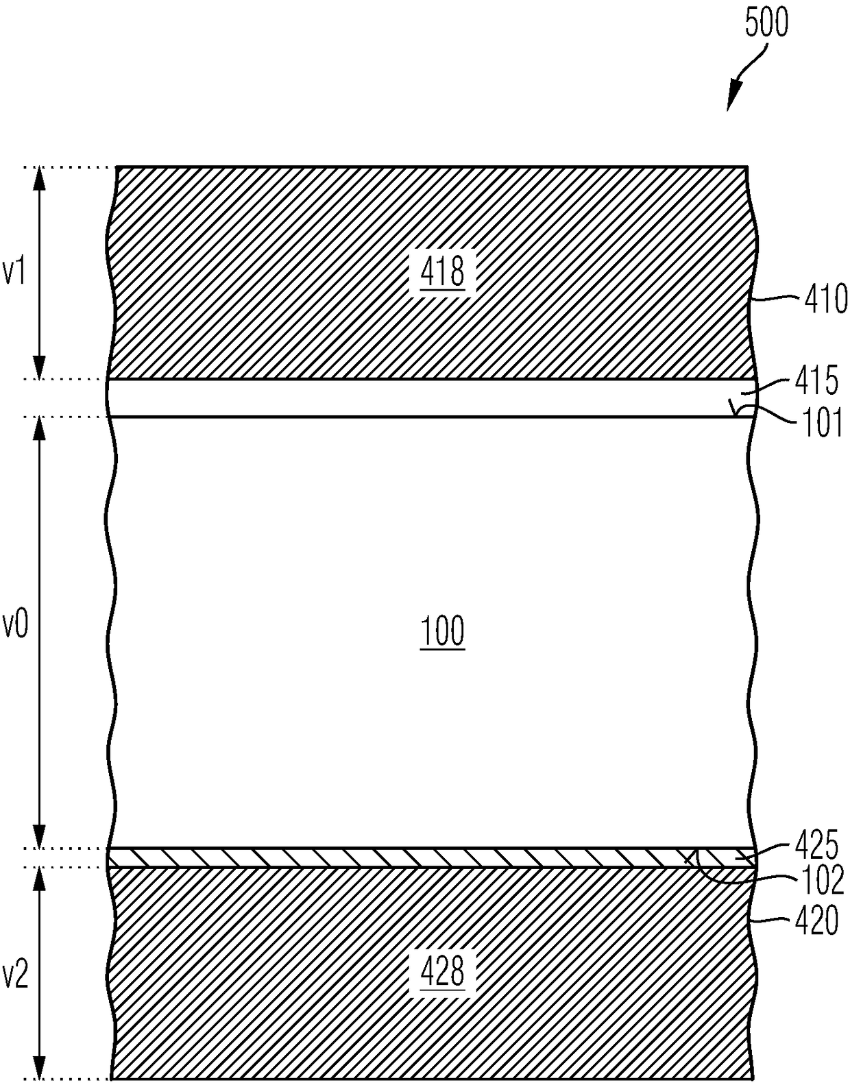
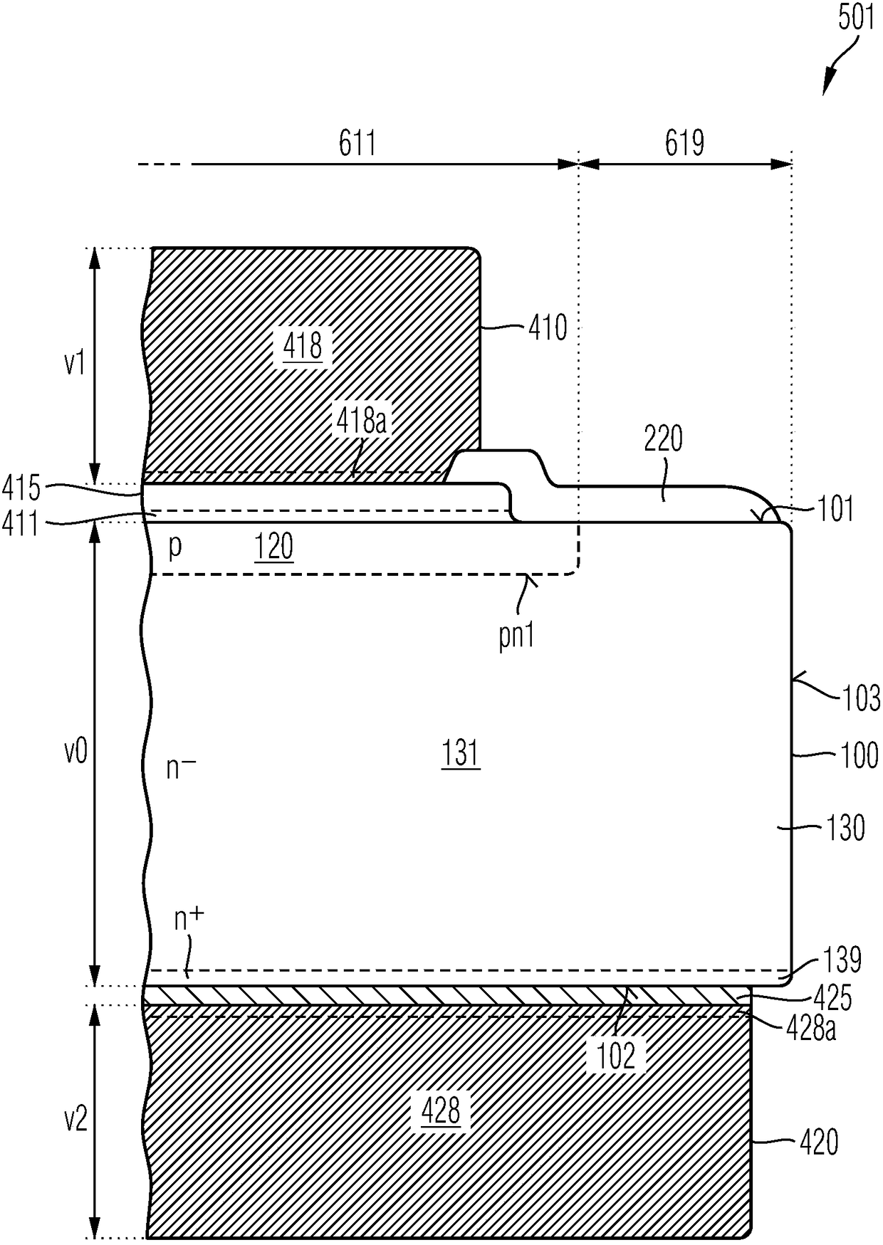
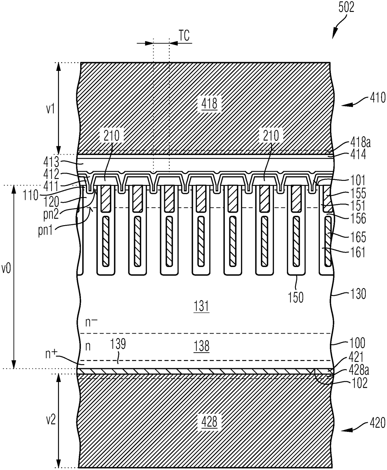
[0043] In the following detailed description, reference is made to the accompanying drawings, which form a part hereof, and in which are shown by way of illustrations specific embodiments in which the invention may be practiced. It is to be understood that other embodiments may be utilized and structural or logical changes may be made without departing from the scope of the present invention. For example, features illustrated or described with respect to one embodiment can be used on or in conjunction with other embodiments to yield a still further embodiment. It is intended that the present invention includes such modifications and variations. These examples were described in specific language, which should not be construed as limiting the scope of the appending claims. The drawings are not drawn to scale and are for illustrative purposes only. If not stated otherwise, corresponding elements are provided with the same reference numerals in the different figures.

[0044] T...


PUM

PropertyMeasurementUnit
Thicknessaaaaaaaaaa
Layer thicknessaaaaaaaaaa

Abstract

A semiconductor device includes a semiconductor layer with a thickness of at most 50 um. The first metallization on the first surface of the semiconductor layer includes a first copper portion havinga first thickness. The second metallization structure on the opposite second surface of the semiconductor layer includes a second copper portion having a second thickness. The total thickness of the first and second thicknesses does not deviate by more than 20% from the die thickness, and the difference between the first and second thicknesses does not exceed 20% of the total thickness.

Description

technical field [0001] The present invention relates to a semiconductor device, a semiconductor switch assembly and a method of manufacturing the semiconductor device. Background technique [0002] In vertical power semiconductor devices such as power semiconductor diodes and MOSFETs (metal oxide semiconductor field effect transistors), the load current flows from the front side of the semiconductor die to the opposite back side. Typically, the metallization layer on the rear side of the power semiconductor device is soldered to the lead frame, and wire bonds connect the metallization layer on the front side with further leads of the device package. One way to reduce the on-state or forward resistance of a power semiconductor device is to reduce the distance between the front and back sides of the semiconductor die. As the thickness of semiconductor die decreases, the processing of semiconductor substrates to obtain thin semiconductor die becomes more complex in terms of ha...

Claims


Application Information

Patent Timeline
IPC IPC(8): H01L23/488H01L21/60
CPCH01L24/27H01L24/28H01L24/30H01L2224/29147H01L2224/2902H01L2224/30181H01L23/482H01L23/49551H01L23/49562H01L23/49575H01L21/6836H01L23/3107H01L23/562H01L21/32139H01L2224/48091H01L29/404H01L29/407H01L21/78H01L29/7813H01L2224/0603H01L2924/00014H01L23/528H01L23/53238H01L23/535H01L23/49527H01L21/4857
Inventor P·加尼策尔M·普埃尔兹
Owner INFINEON TECH AG
Features
  • R&D
  • Intellectual Property
  • Life Sciences
  • Materials
  • Tech Scout
  • Unparalleled Data Quality
  • Higher Quality Content
  • 60% Fewer Hallucinations
Learn More