

Energy-saving lighting device
A lighting device, energy-saving technology, applied in the direction of electrical components, electric solid state devices, circuits, etc., can solve problems such as unfavorable heat dissipation of LED chips, cracking of adhesive layers, and poor edge sealing, so as to facilitate heat dissipation and ensure stability. sexual effect
- Summary
- Abstract
- Description
- Claims
- Application Information
AI Technical Summary
Problems solved by technology
Method used
Image

Examples
no. 1 example
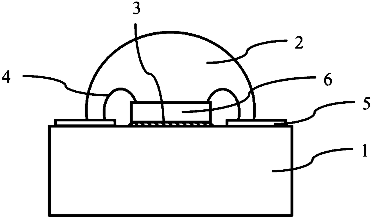
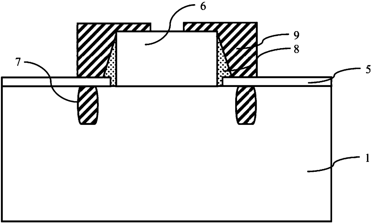
[0017] see image 3 , the energy-saving lighting device of the present invention, which includes a heat dissipation substrate 1, an LED chip 6, a conductive pattern 5, a first insulating material layer 8 and a transparent conductive layer 9; the heat dissipation substrate 1 has a first conductive pattern 5 surface and a second surface opposite to the first surface, the LED chip 6 is fixed to the portion of the first surface of the heat dissipation substrate 1 that is not provided with the conductive pattern 5 through an adhesive layer (not shown) , and there is a gap between the LED chip 6 and the conductive pattern 5, the heat dissipation substrate 1 is also provided with a protruding groove 7 located on the first surface, and the conductive pattern 5 is provided with the Extend into the through hole (not shown) corresponding to the groove; the first insulating material layer 8 covers the side of the LED chip 6 and fills the gap; the transparent conductive layer 9 is electric...
no. 2 example
[0019] see Figure 4 , the present invention also provides another energy-saving lighting device, which includes a heat dissipation substrate 1, an LED chip, a conductive pattern 5, a second insulating material layer 11 and a bonding wire; the heat dissipation substrate 1 has a first conductive pattern 5 One surface and a second surface opposite to the first surface, the LED chip is fixed to the part of the first surface of the heat dissipation substrate 1 that is not provided with the conductive pattern 5 through an adhesive layer (not shown) , and there is a gap between the LED chip 6 and the conductive pattern 5, the heat dissipation substrate 1 is also provided with a protruding groove 10 on the first surface, and the protruding groove 10 is arranged in the gap The LED chip includes a light-emitting middle area 61 and a redundant area 62 surrounding the light-emitting area 61. The side of the redundant area 62 is provided with an annular groove 12, and the annular groove 1...
PUM
 Abstract
Description
Claims
Application Information