Packaging structure of high-density display light source device of LED
A packaging structure and light source technology, which is applied in the direction of electric solid-state devices, semiconductor devices, instruments, etc., can solve the problems of small size, high production cost, and small size of the back pad, so as to improve stability, high production efficiency, and simplify complexity sexual effect
- Summary
- Abstract
- Description
- Claims
- Application Information
AI Technical Summary
Problems solved by technology
Method used
Image
Examples
Embodiment 1
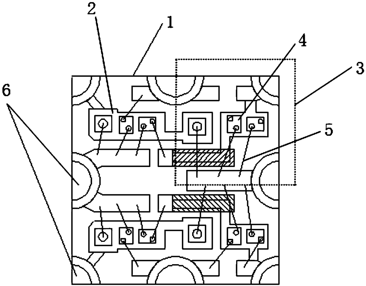
[0038] A light-emitting unit 3 with 2 rows*2 columns is provided by adopting copper foil hole cutting technology.
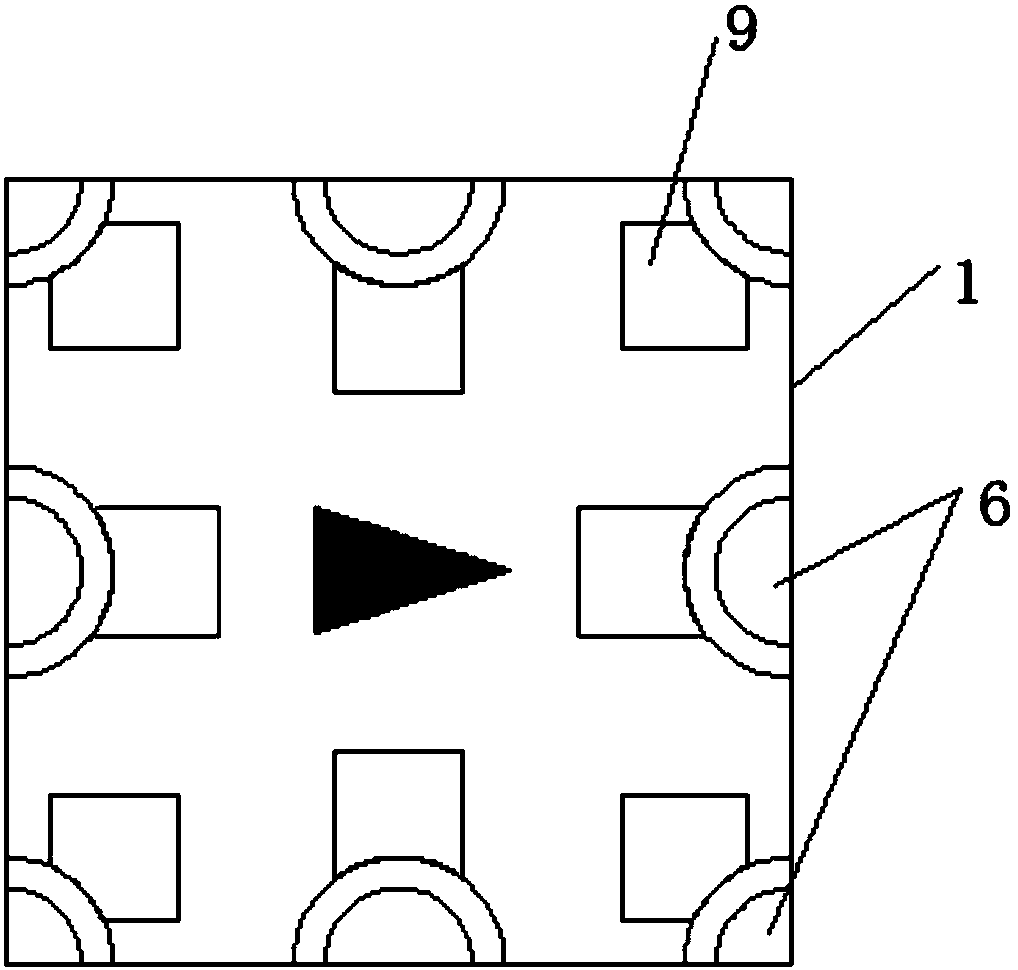
[0039] Such as figure 1 , 2 As shown, the front circuit line of the substrate 1 is connected to the back circuit line 2 through the copper wall of the 1 / 4 circular cut hole or 1 / 2 circular cut hole on the edge to realize the circuit connection. For the setting of the conductive hole 6, see figure 1 and figure 2 . There are 4 light-emitting units (that is, 2 rows and 2 columns) on the front pad of the substrate 11, and the distance between the four light-emitting units is 1mm; 8 pads 9 are set on the back, respectively controlling the negative electrodes of the red light chips in each row (2 rows in total) , the negative electrodes of the green chips in each row (2 rows in total), the negative electrodes of the blue chips in each row (2 rows in total), and the common positive electrodes in each column (2 columns in total).
[0040] Each light-emitting unit 3 ...
Embodiment 2
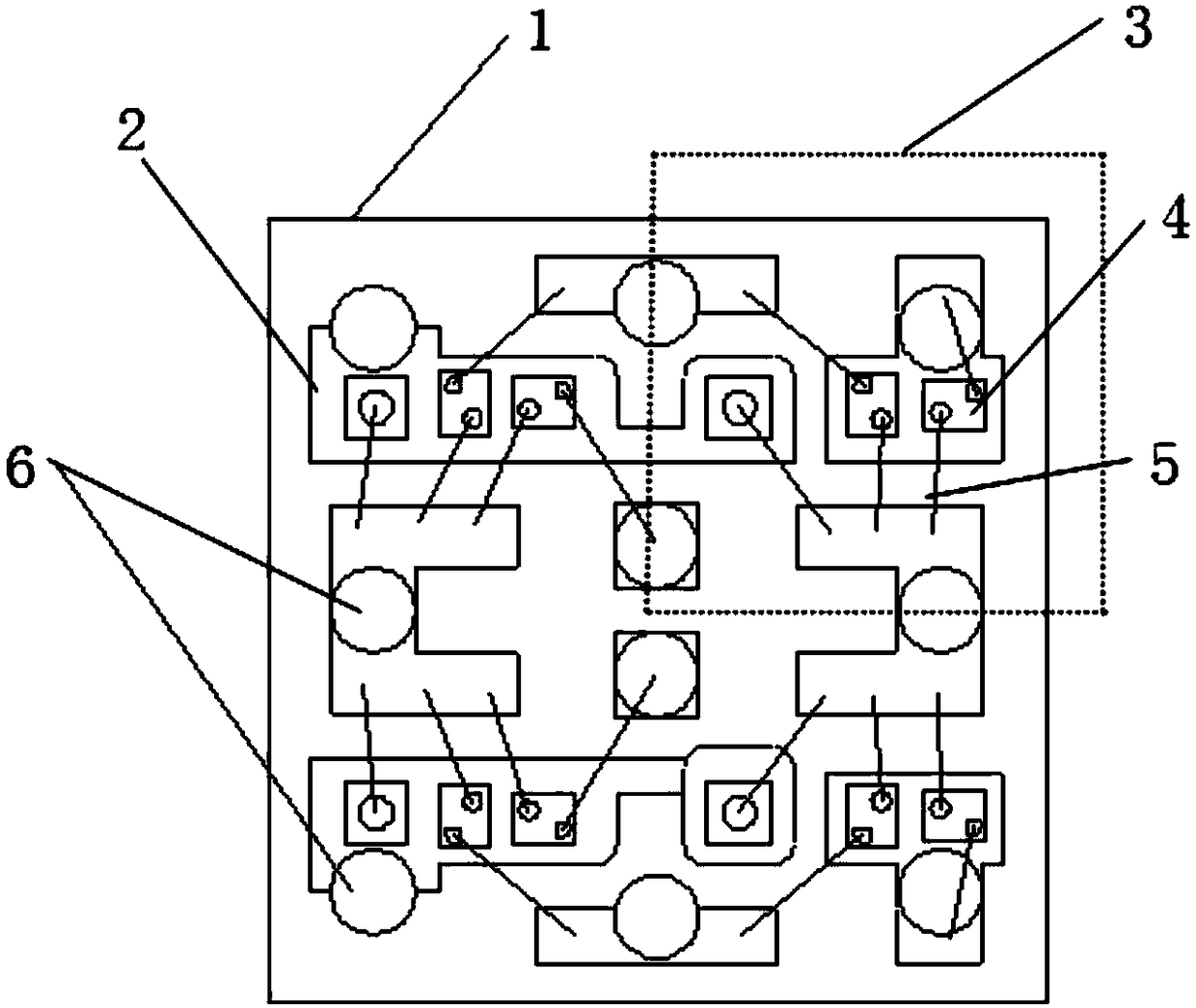
[0045] The second embodiment provides a light-emitting unit 3 with 2 rows*2 columns that adopts a copper pillar via technology structure.
[0046] Such as image 3 , 4 As shown, the circuit line 2 on the front side of the substrate 1 is connected to the line on the back side through the copper pillar hole to realize the circuit connection. image 3 and Figure 4 . 4 light-emitting units 3 (that is, 2 rows and 2 columns) are arranged on the front pad of the substrate 1, and the distance between the 4 light-emitting units 3 is 1 mm; 8 pads 9 are arranged on the back, respectively controlling the negative electrodes of the red light chips in each row (a total of 2 rows), the negative electrodes of the green chips in each row (2 rows in total), the negative electrodes of the blue chips in each row (2 rows in total), and the common positive electrodes in each column (2 columns in total).
[0047] Each light-emitting unit 3 is provided with 3 chips, which are respectively 1 red ...
Embodiment 3
[0052] Such as Figure 5 , 6 As mentioned above, on the basis of the second embodiment, the third embodiment adopts the inkjet printing technology to perform inkjet treatment on the metal pad after the wire bonding, the ink is black ink, and the thickness of the ink layer 8 is 50-150um. The surface contrast of the device treated by the ink-jet technology is significantly improved, and the thick ink can prevent light crossing and mutual interference among the light-emitting units 3 and improve the fidelity of the displayed color. Seal the semi-products after inkjet with transparent glue to protect the light-emitting chip 4. The transparent glue can be realized through traditional molding and dispensing processes, or through inkjet printing, 3D printing and other technologies. The thickness of the glue can be 0.3-0.8 mm.
PUM
 Abstract
Description
Claims
Application Information


