Light emitting diode chip and manufacturing method thereof

A technology of light-emitting diodes and manufacturing methods, which is applied in the direction of electrical components, circuits, semiconductor devices, etc., can solve the problems that the front light emission of LED chips needs to be improved, and achieve the effect of increasing front light emission

Active Publication Date: 2018-05-29
HC SEMITEK ZHEJIANG CO LTD
View PDF6 Cites 15 Cited by
  • Summary
  • Abstract
  • Description
  • Claims
  • Application Information

AI Technical Summary

Problems solved by technology

[0006] In order to solve the problem that the front light output of the LED chip in the prior art still needs to be improved, the embodiment of the present invention provides a light emitting diode chip and its manufacturing method

Method used


Image

  • Light emitting diode chip and manufacturing method thereof
  • Light emitting diode chip and manufacturing method thereof
  • Light emitting diode chip and manufacturing method thereof

Examples


Embodiment 1

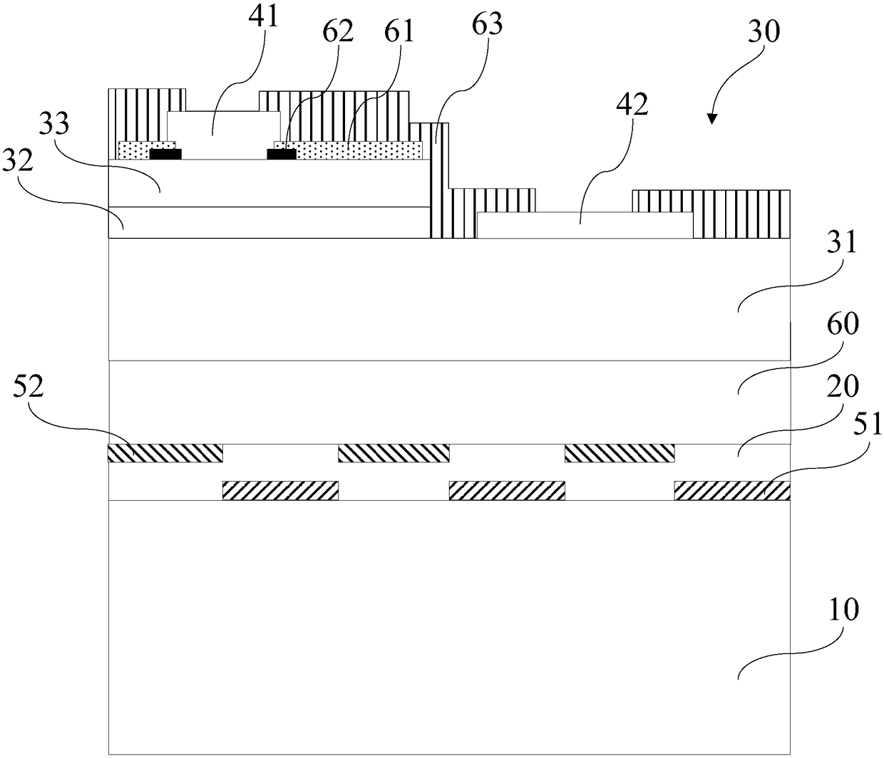
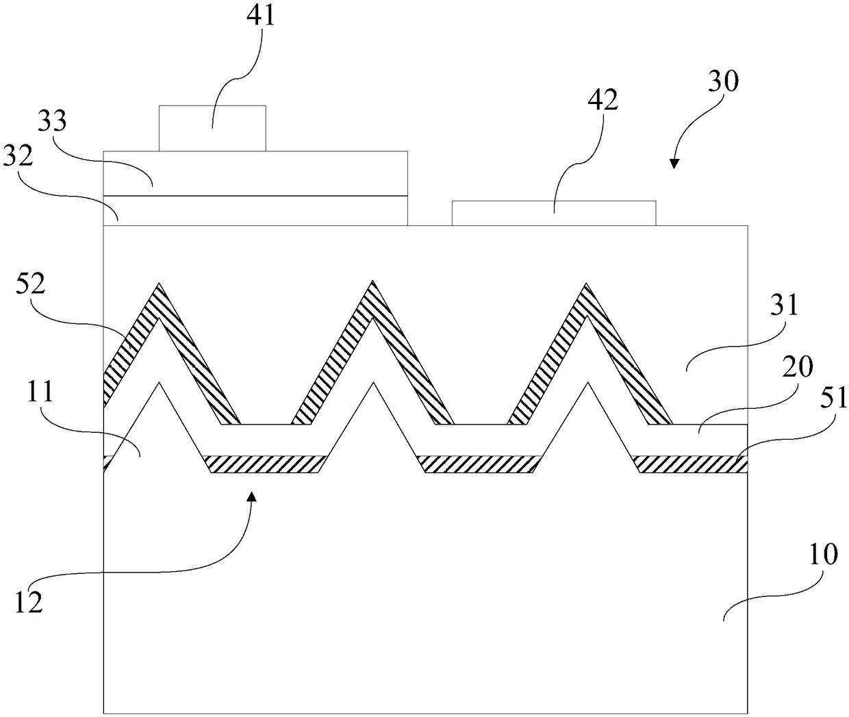
[0050] An embodiment of the present invention provides a light emitting diode chip, figure 1 is a schematic diagram of the structure of a light-emitting diode chip, see figure 1 , the LED chip includes a substrate 10 , a buffer layer 20 , an N-type semiconductor layer 31 , a multiple quantum well layer 32 , a P-type semiconductor layer 33 , a P-type electrode 41 and an N-type electrode 42 . The buffer layer 20, the N-type semiconductor layer 31, the multiple quantum well layer 32, and the P-type semiconductor layer 33 are sequentially stacked on one surface of the substrate 10, and the P-type semiconductor layer 33 is provided with a groove extending to the N-type semiconductor layer 31 30 , the N-type electrode 42 is disposed on the N-type semiconductor layer 31 in the groove 30 , and the P-type electrode 41 is disposed on the P-type semiconductor layer 33 .

[0051] In this embodiment, the LED chip further includes a first reflective layer 51 and a second reflective layer 5...

Embodiment 2

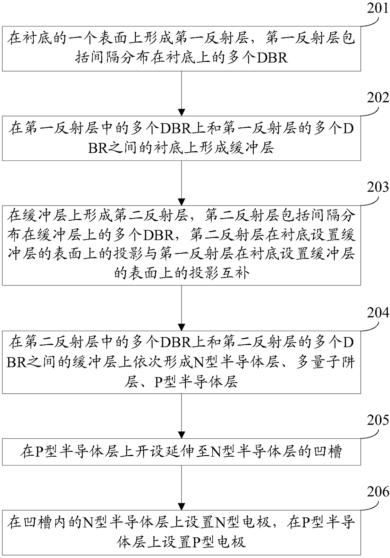
[0084] An embodiment of the present invention provides a method for manufacturing a light emitting diode chip, which is suitable for manufacturing the light emitting diode chip provided in the first embodiment. image 3 For a flowchart of the method, see image 3 , the production method includes:

[0085] Step 201: forming a first reflective layer on one surface of a substrate, the first reflective layer comprising a plurality of DBRs distributed on the substrate at intervals.

[0086] Optionally, the surface of the substrate on which the first reflective layer is provided may include a plurality of protrusions, the plurality of protrusions are arranged in an array, and a recess is provided between two adjacent protrusions.

[0087] In the above implementation manner, a plurality of DBRs in the first reflective layer may be disposed on the depressed portion.

[0088] Preferably, the thickness of the first reflective layer may be smaller than the height of the raised portion,...


PUM


Abstract

The invention discloses a light emitting diode chip and a manufacturing method thereof, belonging to the technical field of semiconductors. The chip includes a substrate, a buffer layer, an N-type semiconductor layer, a multiple quantum well layer, a P-type semiconductor layer, a P-type electrode, an N-type electrode, a first reflective layer and a second reflective layer. Each of the first reflective layer and the second reflective layer comprises a plurality of DBRs spaced in the same plane, the plurality of DBRs in the first reflective layer are disposed between the substrate and the bufferlayer, and the plurality of DBR layers in the second reflective layer are disposed between the buffer layer and the N-type semiconductor layer. The projection of the first reflective layer on the surface of the substrate provided with the buffer layer is complementary to the projection of the second reflective layer on the surface of the substrate provided with the buffer layer. The light emitting diode chip can effectively prevent the light emitted to the substrate from being emitted from the side of the substrate, greatly increasing the front-side light emission of the LED chip, and the lattice characteristics of the substrate are transmitted to the N-type semiconductor layer through the buffer layer to avoid affecting the N-type semiconductor layer and the subsequent semiconductor layer growth quality.

Description

technical field [0001] The invention relates to the technical field of semiconductors, in particular to a light emitting diode chip and a manufacturing method thereof. Background technique [0002] Light Emitting Diode (English: Light Emitting Diode, referred to as: LED) is a new generation of solid-state lighting source with high efficiency, environmental protection and green, which has the advantages of low voltage, low power consumption, small size, light weight, long life and high reliability. quickly and widely used. [0003] The core part of the LED is the chip. The existing LED chip includes a substrate, a buffer layer, an N-type semiconductor layer, a multi-quantum well layer, a P-type semiconductor layer, a current blocking layer, a transparent conductive layer, a P-type electrode, an N-type electrode, A passivation layer and a distributed Bragg reflector (English: Distributed Bragg Reflection, DBR for short). The DBR is arranged on the first surface of the substr...

Claims


Application Information

Patent Timeline
Patent Type & Authority Applications(China)
IPC IPC(8): H01L33/10H01L33/12H01L33/00
Inventor 兰叶顾小云黄龙杰王江波
Owner HC SEMITEK ZHEJIANG CO LTD
Why Eureka
Try Eureka