Supercharge Your Innovation With Domain-Expert AI Agents!

Degassing chambers and semiconductor processing equipment

A gas chamber and cavity technology, which is applied in the field of degassing chambers and semiconductor processing equipment, can solve the problems that the temperature of the chamber 1 cannot be the same, the degassing effect of the workpiece S to be processed is different, and the inner wall becomes dirty, so as to eliminate the heating effect of effect

Active Publication Date: 2020-10-16
BEIJING NAURA MICROELECTRONICS EQUIP CO LTD
View PDF5 Cites 0 Cited by
  • Summary
  • Abstract
  • Description
  • Claims
  • Application Information

AI Technical Summary

Problems solved by technology

[0004] However, there are at least the following problems in the prior art: since the inner wall of the cavity 1 is generally made of metal material, the light emitted by the halogen lamp 4 can pass through the transparent dielectric window 2 to the inner wall of the cavity 1, and the cavity The inner wall of 1 will reflect the light, and the reflected light can also heat the workpiece S to be processed. As the number of pieces of workpiece S to be processed increases, the impurity gas baked out by the degassing process adheres to the surface of chamber 1 The inner wall makes the inner wall of the chamber 1 dirty, causing the reflection of the light on the inner wall of the chamber 1 to be weakened. Therefore, the light reflected by the inner wall of the chamber 1 in multiple processes is not the same (that is, unstable), so It is impossible to make the temperature in the chamber 1 the same during multiple processes. If the same process time is used, the degassing effect of the workpiece S to be processed will be different in multiple processes, thereby affecting the subsequent process quality; if the degassing effect is the same , the process time required for multiple processes is different, which makes the process operation complicated

Method used


Image

  • Degassing chambers and semiconductor processing equipment
  • Degassing chambers and semiconductor processing equipment
  • Degassing chambers and semiconductor processing equipment

Examples


Embodiment 1

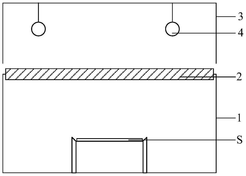
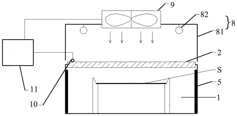
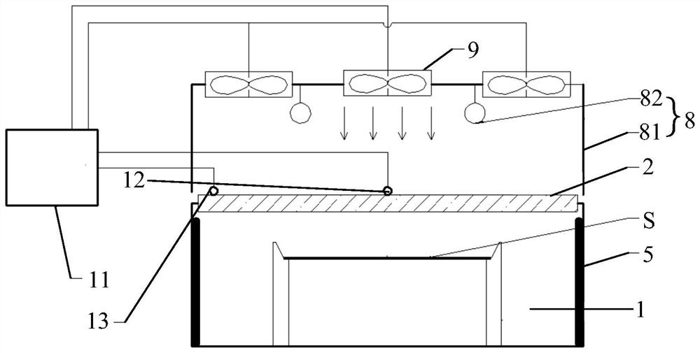
[0026] Please refer to Figure 2 to Figure 5 , the present embodiment provides a degassing chamber, including: a chamber 1 and a heating device 8 arranged on the upper part of the chamber 1, the heating device 8 heats the workpiece S placed in the chamber 1 by emitting light ; The inner wall and / or inner bottom wall of the cavity 1 is provided with an anti-reflection structure, which is used to weaken or eliminate the reflection of light on the inner wall and / or inner bottom wall of the cavity 1 .

[0027] Please refer to figure 2 , a dielectric window 2 is installed on the top wall of the cavity 1, that is, the dielectric window 2 seals the top wall of the cavity 1, so that the cavity 1 forms a closed vacuum chamber; generally, the dielectric window 2 is made of quartz material It is made in a transparent state, so the light emitted by the heating device 8 above the dielectric window 2 can pass through the transparent dielectric window 2 and irradiate the workpiece S in the...

Embodiment 2

[0055] This embodiment provides a semiconductor processing device, including the degassing chamber of Embodiment 1.

[0056] In the semiconductor processing equipment of this embodiment, since an anti-reflection structure is provided on the inner side wall and / or the inner bottom wall of the cavity, the reflection of the light emitted by the heating device by the side wall of the degassing chamber can be weakened or even eliminated, thereby eliminating The heating effect of the heat generated by the reflected light on the workpiece to be processed is eliminated, so that the temperature of the workpiece to be processed no longer decreases as the inner wall of the degassing chamber becomes dirty.


PUM


Abstract

The invention provides a degassing chamber and semiconductor processing apparatus. The degassing chamber comprises a cavity and a heating device disposed on the upper portion of the cavity, wherein the heating device heats a to-be-processed object placed in the cavity by means of emitted light rays; and the inner side wall and / or the inner bottom wall of the cavity is provided with an anti-reflection structure for reducing or eliminating reflection of light rays by the inner side wall and / or the inner bottom wall of the cavity. The semiconductor processing equipment comprises the degassing chamber. The degassing chamber can reduce or even eliminate the reflection of the light rays emitted from the heating device by the inner side wall and / or the inner bottom wall of the degassing chamber,so that the heating effect on the to-be-processed object caused by heat generated by the reflected light rays is eliminated, and the temperature of the to-be-processed object is no longer reduced as the inner walls of the degassing chamber becomes dirty.

Description

technical field [0001] The invention belongs to the technical field of semiconductor equipment manufacturing, and in particular relates to a degassing chamber and semiconductor processing equipment. Background technique [0002] In the semiconductor equipment integration system, there are mainly three types of modules according to their functions, including degassing process modules, pre-cleaning process modules and deposition process modules. Among them, the degassing process module is the first process module in the whole process flow. It is mainly to degas the workpiece to be processed, so as to remove the impurity gas remaining on the surface or inside of the workpiece S to be processed. These impurity gases cannot appear in the subsequent process chamber. Indoor, otherwise it will affect the performance of semiconductor devices. [0003] In the prior art, the degassing process module bakes and degasses the workpiece through three methods, one is heating with a halogen ...

Claims


Application Information

Patent Timeline
Patent Type & Authority Patents(China)
IPC IPC(8): H01L21/67
CPCH01L21/67011H01L21/67115
Inventor 郑金果
Owner BEIJING NAURA MICROELECTRONICS EQUIP CO LTD
Features
  • R&D
  • Intellectual Property
  • Life Sciences
  • Materials
  • Tech Scout
  • Unparalleled Data Quality
  • Higher Quality Content
  • 60% Fewer Hallucinations
Learn More