Display panel

A display panel and display area technology, applied in the direction of instruments, nonlinear optics, optics, etc., can solve the problems of energy consumption, excessive resistance and capacitance load, etc., and achieve the effect of reducing the size

Inactive Publication Date: 2018-06-08
HKC CORP LTD
View PDF7 Cites 6 Cited by
  • Summary
  • Abstract
  • Description
  • Claims
  • Application Information

AI Technical Summary

Problems solved by technology

In the GOA type liquid crystal display panel in the prior art, liquid crystal molecules are filled between the gate drive circuit of the GOA type liquid crystal display panel and the common electrode of the liquid crystal display panel. Since the gate drive circuit of the GOA type liquid crystal display panel contains active Switching element TFT (Thin Film Transistor, Thin Film Transistor), capacitance will be generated between TFT and common electrode, which will easily lead to the problem of excessive resistance and capacitance load generated on the gate drive circuit, and excessive energy consumption

Method used


Image

  • Display panel
  • Display panel
  • Display panel

Examples


Embodiment Construction

[0022] The following will clearly and completely describe the technical solutions in the embodiments of the present invention with reference to the accompanying drawings in the embodiments of the present invention. Obviously, the described embodiments are only some, not all, embodiments of the present invention. Based on the embodiments of the present invention, all other embodiments obtained by persons of ordinary skill in the art without creative efforts fall within the protection scope of the present invention.

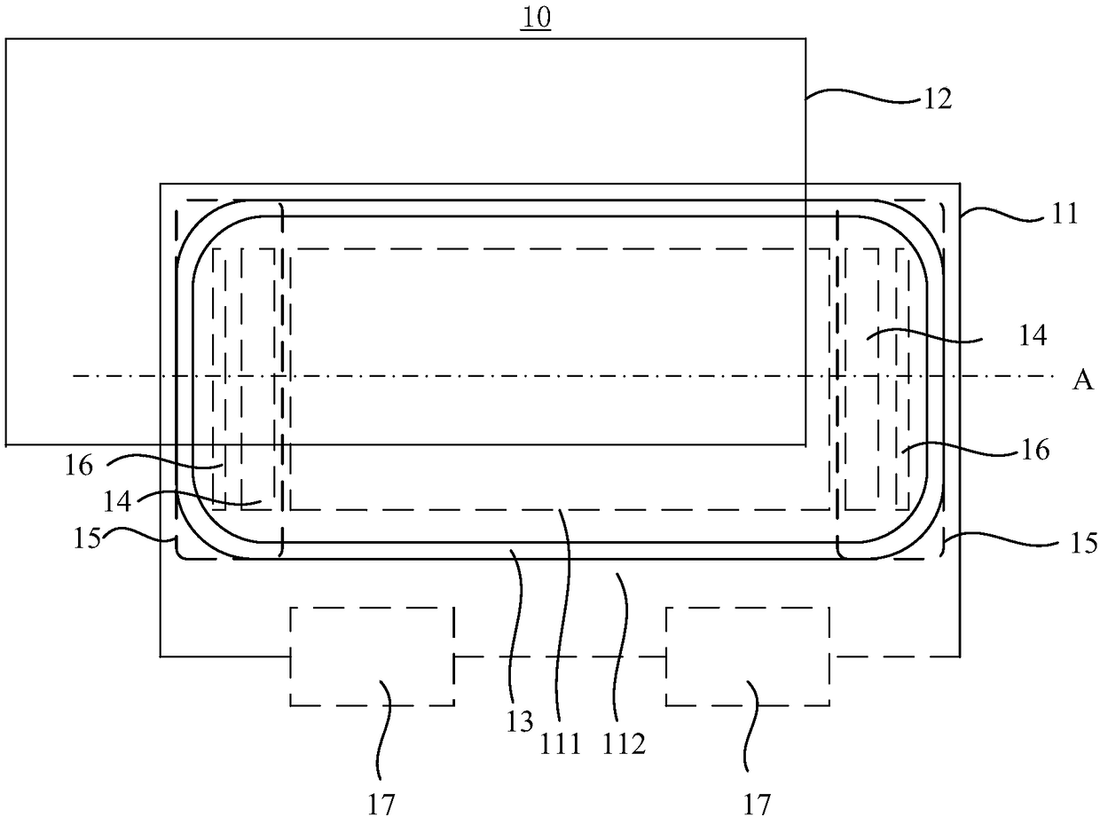
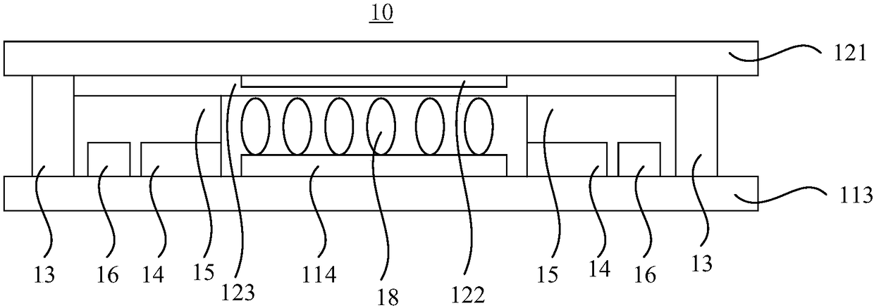
[0023] Such as Figure 1A A display panel 10 provided for an embodiment of the present invention mainly includes: an active switch array substrate 11, an opposing substrate 12, a sealant 13, an array substrate gate driver (GOA) 14, a spacer 15, and a signal transmission bus 16 and source driver chip 17. Among them, the active switch array substrate 11 includes a display area 111 and a peripheral area 112 surrounding the display area 111; the opposite substrate 12 i...


PUM


Abstract

The embodiment of the invention discloses a display panel. The display panel comprises an active switch array substrate, an opposite substrate, frame glue, a display medium layer, an array substrate grid driver and a separator; the active switch array substrate comprises a display area and a peripheral zone surrounding the display area, the opposite substrate is arranged to be opposite to the active switch array substrate, the frame glue is arranged between the active switch array substrate and the opposite substrate and located in the peripheral zone so as to form a containing space togetherwith the active switch array substrate and the opposite substrate, the display medium layer is located in the containing space, the array substrate grid driver is arranged in the peripheral zone of the active switch array substrate and located in the containing space, the separator is arranged between the active switch array substrate and the opposite substrate and used for separating the displaymedium layer in the containing space and the array substrate grid driver. Accordingly, the size of resistance and capacitance load generated on the array substrate grid driver can be effectively lowered.

Description

technical field [0001] The present invention relates to the field of display technology, in particular to a display panel. Background technique [0002] The process architecture of the display panel can be divided into SOC (System on chip) and GOA (Gate driver on array, array substrate gate driver) according to the design scheme of the gate drive. SOC is to drive the gate through the external integrated chip. Realized, the gate drive of the GOA is realized by setting a gate drive circuit between the array substrate and the color filter substrate of the display panel. Compared with SOC design, GOA can achieve narrower frame and has lower cost. GOA products will be the mainstream trend in the future. In the GOA type liquid crystal display panel in the prior art, liquid crystal molecules are filled between the gate drive circuit of the GOA type liquid crystal display panel and the common electrode of the liquid crystal display panel. Since the gate drive circuit of the GOA typ...

Claims


Application Information

Patent Timeline
Patent Type & Authority Applications(China)
IPC IPC(8): G02F1/1339G02F1/1345
CPCG02F1/13394G02F1/13454G02F1/133514G02F1/1339
Inventor 单剑锋
Owner HKC CORP LTD
Why Eureka
Try Eureka