Interactive multi-step physical synthesis

A technology of processors and processing resources, applied in electrical digital data processing, special data processing applications, instruments, etc., and can solve problems such as long delays

Active Publication Date: 2018-06-08
XILINX INC
View PDF7 Cites 5 Cited by
  • Summary
  • Abstract
  • Description
  • Claims
  • Application Information

AI Technical Summary

Problems solved by technology

Placing connected elements close to each other also generally improves the performance of the circuit, since long interconnect paths are associated with excess capacitance and resistance, resulting in longer delays

Method used


Image

  • Interactive multi-step physical synthesis
  • Interactive multi-step physical synthesis
  • Interactive multi-step physical synthesis

Examples


Embodiment Construction

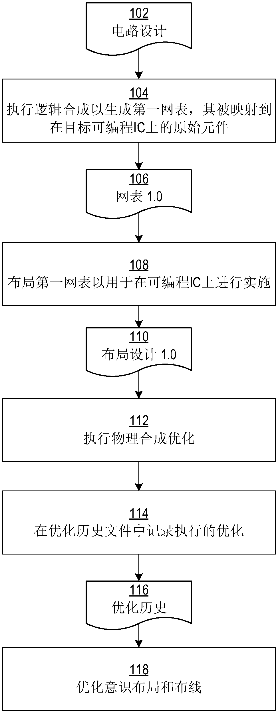
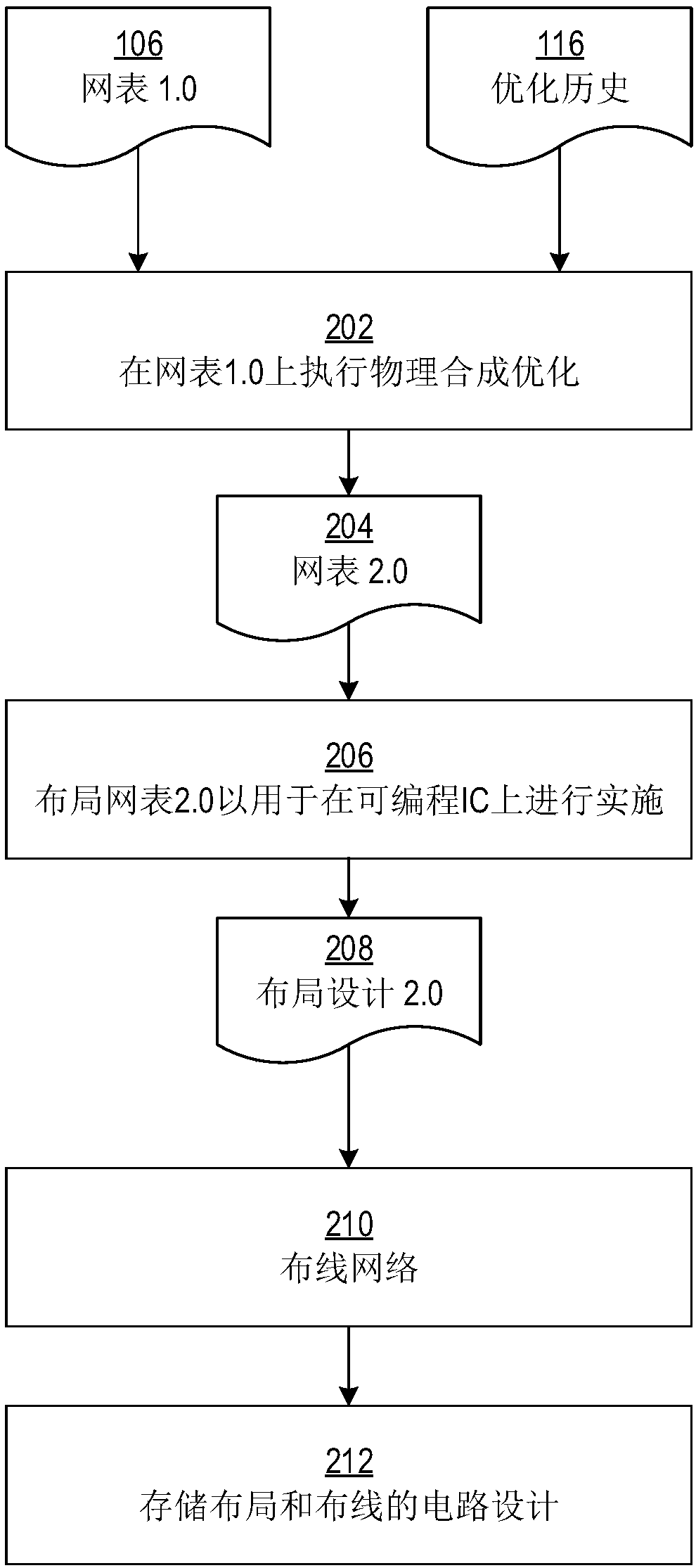
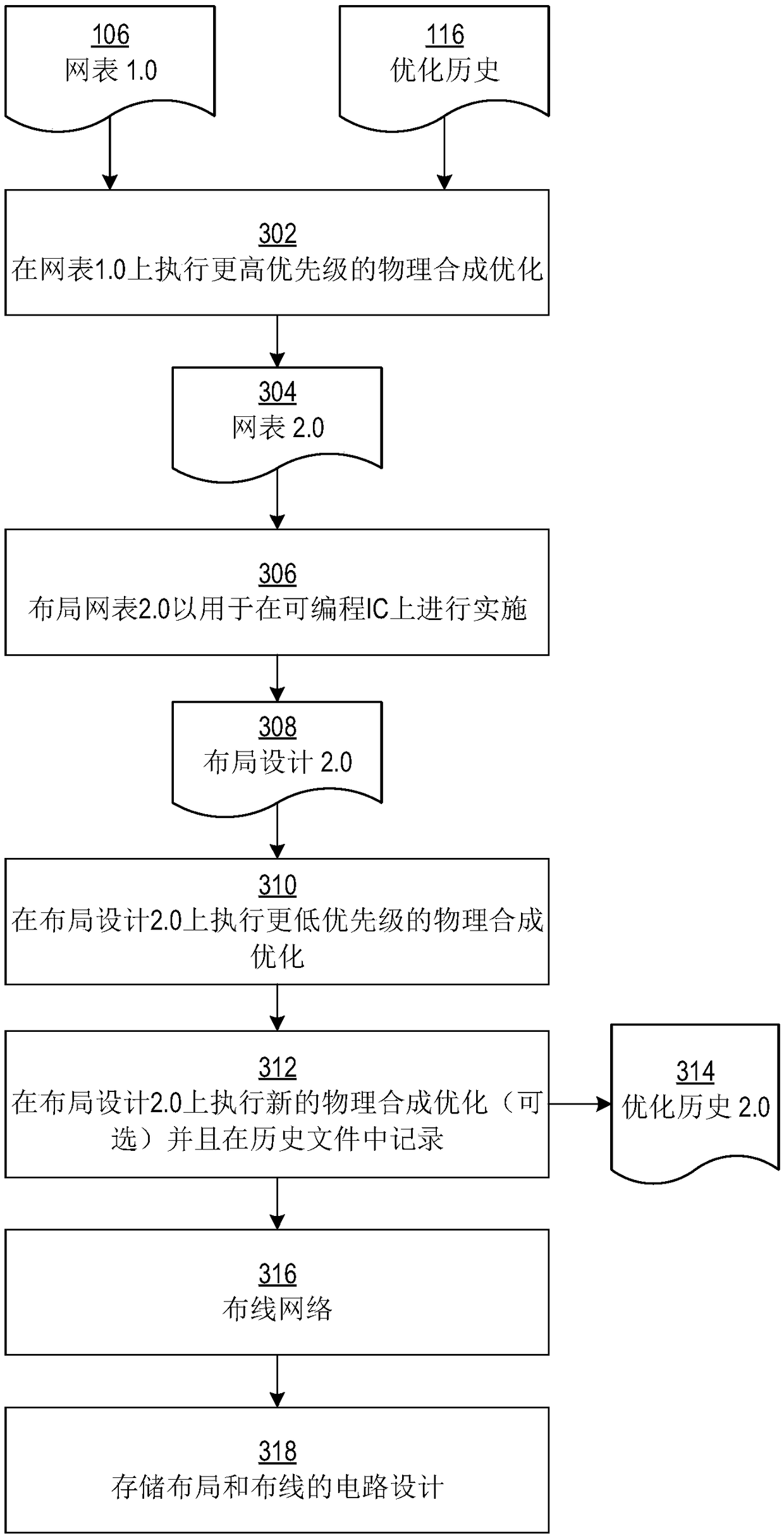
[0034]When routing a circuit design, it is possible to test a large number of different routings before finding a routing solution that meets the timing requirements of the design. Routing time may be extended due to non-optimal placement. In existing place and route techniques, physical synthesis optimization is performed after placement, and then the optimized design is routed. For example, physical synthesis optimizations may be performed to improve timing, noise margin, die area, and / or power usage. Physical synthesis optimization converts the physical elements of a circuit design into different (but logically identical) physical elements that meet the design requirements.

[0035] Due to changes made to the circuit design during physical synthesis optimization, the layout may no longer be optimal for the modified circuit design. Since physical composition optimization is performed after layout, layout does not take into account changes from optimization. As a result, r...


PUM


Abstract

In one embodiment of the invention, a processor-implemented method is provided for placing and routing a circuit design (102). A first netlist is generated for a circuit design. Placement is performed(108) for the first netlist (106) on a target IC to produce a first placed design (1 10). A set of optimizations are performed (1 12) on the first placed design. The set of optimizations are recorded(1 14) in an optimization history file (1 16). One or more optimizations specified in the optimization history file are performed (1 18/202) on the first netlist to produce a second netlist that is different than the first netlist. Placement is performed (206) for the second netlist on the target IC to produce a second placed design (208) that is different than the first placed design. Nets of the second placed design are routed (210) to produce a placed and routed circuit design.

Description

technical field [0001] The present disclosure generally relates to placement, routing, and timing closure of resources in programmable integrated circuits. Background technique [0002] Programmable logic devices (PLDs) are integrated circuits (ICs) used to implement digital logic operations based on user-configurable inputs. Example PLDs include complex programmable logic devices (CPLDs) and field programmable gate arrays (FPGAs). CPLDs typically contain multiple functional blocks based on a programmable logic array (PLA) architecture with sum-of-products logic. A configurable interconnect matrix transfers signals between functional blocks. [0003] An example FPGA includes an array of configurable logic blocks (CLBs) and rings or columns of programmable input / output blocks (IOBs). CLBs and IOBs are connected to each other through programmable interconnect structures (routing resources). CLBs, IOBs and interconnect structures are typically programmed by loading a stream...

Claims


Application Information

Patent Timeline
Patent Type & Authority Applications(China)
IPC IPC(8): G06F17/50
CPCG06F30/34G06F30/392G06F30/394G06F30/398G06F2119/12G06F2119/06
Inventor R·阿加沃尔Z·王R·刘S·达斯
Owner XILINX INC
Why Eureka
Try Eureka