Array substrate, drive method thereof and display device
An array substrate and substrate technology, applied in optics, instruments, electrical components, etc., can solve the problems of lower production capacity of display panels and lower utilization rate of display panels, and achieve the effect of improving utilization rate and reducing production costs
- Summary
- Abstract
- Description
- Claims
- Application Information
AI Technical Summary
Problems solved by technology
Method used
Image


Examples
Embodiment 1
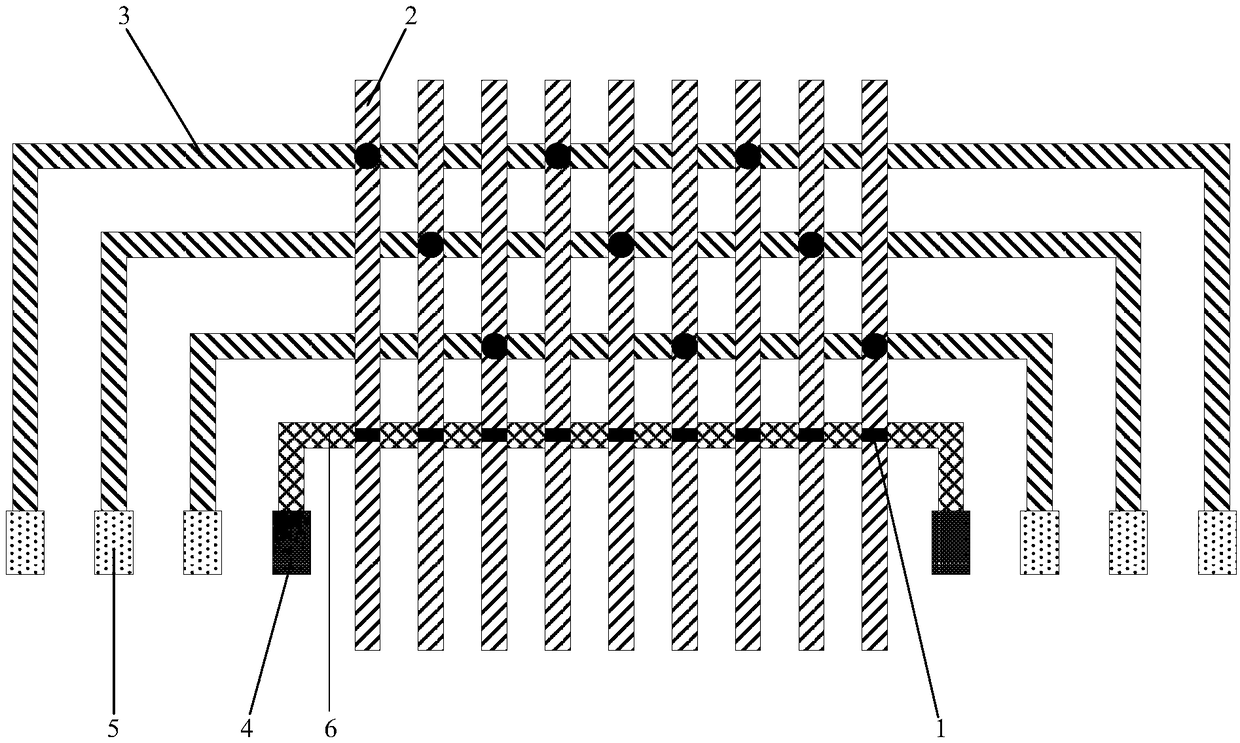
[0031] Such as figure 1 As shown, this embodiment provides an array substrate, which includes: a substrate, a plurality of signal lines 2, a shorting bar 3, and a switch unit 1; specifically, a plurality of signal lines 2 are arranged on the substrate; each signal line 2 is connected to The corresponding shorting bar 3 is connected to each signal line 2 with a switch unit 1 ; wherein, the switching unit 1 is used to control whether the signal line 2 connected to it is electrically connected to the shorting bar 3 .
[0032] Since each signal line 2 in this embodiment is connected to a switch unit 1, and when the switch unit 1 is in a closed state, the signal line 2 connected to the switch unit 1 will be electrically connected to the short-circuit bar 3, so that the detection The signal is input to the signal line 2 connected to the short-circuit bar 3 through the short-circuit bar 3, so that the pixel unit connected to the signal line 2 can display, and the display condition of...
Embodiment 2
[0034] Such as figure 1 As shown, this embodiment provides an array substrate, which includes: a base, a plurality of signal lines 2 , a shorting bar 3 , a switch unit 1 , and a control unit 4 . Wherein, a plurality of signal lines 2 are arranged on the substrate; each signal line 2 is connected to its corresponding short-circuit bar 3, and each signal line 2 is connected with a switch unit 1; the control unit 4 communicates with each switch through a control line 6 The unit 1 is connected to control the switching on and off of the switching unit 1 , so as to control whether the signal line 2 connected to the switching unit 1 is electrically connected to the shorting bar 3 .
[0035] Specifically, the control unit 4 applies a turn-on voltage to each switch unit 1 on the same control line 6 to turn on the switch unit 1. At this time, the signal line 2 connected to the switch unit 1 will be electrically connected to the short-circuit bar 3, so that the detection The signal is i...
Embodiment 3
[0049] This embodiment provides a display device, which includes the array substrate in Embodiment 1 or Embodiment 2. Wherein, the display device in this embodiment can be any product or component with a display function, such as a liquid crystal panel, an electronic paper, an OLED panel, a mobile phone, a tablet computer, a television set, a monitor, a notebook computer, a digital photo frame, and a navigator.
PUM
 Abstract
Description
Claims
Application Information
PatSnap Eureka turns technology decisions into work you can execute. Powered by our Innovation Knowledge Graph, it runs expert workflows across engineering, life sciences, materials and intellectual property. Get your review-ready output in minutes.


