Graded gold finger and manufacturing method of optical module PCB comprising graded gold finger

A PCB board and gold finger technology, applied in the field of optical module PCB board production, can solve problems such as functional impact and corrosion, and achieve the effects of improving quality, avoiding attacks, and reducing exposed copper area.

Inactive Publication Date: 2018-06-15
深圳欣强智创电路板有限公司
View PDF9 Cites 9 Cited by
  • Summary
  • Abstract
  • Description
  • Claims
  • Application Information

AI Technical Summary

Problems solved by technology

[0004] The traditional graded gold finger structure optical module printed circuit board adopts finger segmentation, the lead wire is as large as the finger, and the method of etching the lead wire between the fingers after making the electric gold fin

Method used


Image

  • Graded gold finger and manufacturing method of optical module PCB comprising graded gold finger
  • Graded gold finger and manufacturing method of optical module PCB comprising graded gold finger

Examples


Embodiment Construction

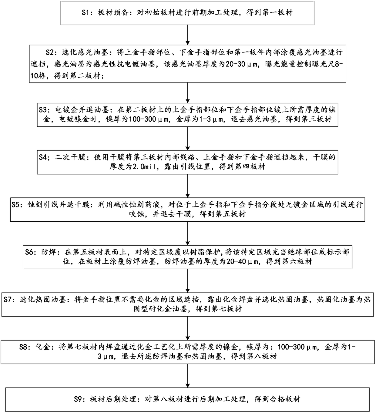
[0038] In order to make the object, technical solution and advantages of the present invention clearer, the present invention will be further described in detail below in conjunction with the accompanying drawings and embodiments. It should be understood that the specific embodiments described here are only used to explain the present invention, not to limit the present invention.

[0039] To achieve the above object, the technical scheme of the present invention is as follows:

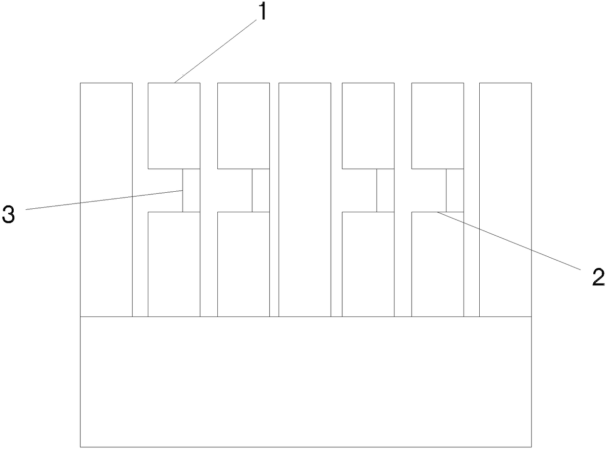
[0040] see Figure 1-2 As shown, the present invention provides a method for manufacturing a graded gold finger and an optical module PCB board including the graded gold finger, specifically comprising:

[0041] A graded gold finger, the graded gold finger includes an upper gold finger 1, a lower gold finger 2, and a lead wire 3, and the upper gold finger 1, the lower gold finger 2, and the lead wire 3 are all rectangular, and it is characterized in that the lead wire 3 is arranged between the upper...


PUM

PropertyMeasurementUnit
Thicknessaaaaaaaaaa
Thicknessaaaaaaaaaa

Abstract

The invention discloses a graded gold finger. The graded gold finger comprises upper golden fingers, lower gold fingers, and leads, wherein the upper gold fingers, the lower gold fingers, and the leads are all rectangular. The graded gold finger is characterized in that the leads are arranged between the upper gold fingers and the lower gold fingers; the upper sides and lower sides of the lead arefixedly connected with the upper gold fingers and the lower gold fingers respectively; and the width of the leads is smaller than the width of the gold fingers. The invention also discloses a manufacturing method of an optical module PCB comprising the graded golden finger. The method comprises the following steps of: plate preparation; selective electroless nickel immersion gold of photosensitive ink; electroplating gold and ink removal; secondary dry film treatment; lead etching and dry film removal; solder masking; selective electroless nickel/immersion gold of heat-set ink; electroless nickel/immersion gold; and plate after-treatment. The method is based on the structural characteristics of the above graded gold finger. With the method adopted, the problem of the falling off of soldermasking sites of a finished board can be solved; and the quality of a PCB manufactured by the method can be further improved.

Description

technical field [0001] The invention belongs to the field of PCB board manufacture, and in particular relates to a method for manufacturing a graded golden finger and an optical module PCB board including the golden finger. Background technique [0002] On the printed circuit board near the edge of the board, there are many rectangular metal contacts arranged in rows, and the metal contacts are formed by electroplating a layer of nickel gold on the copper surface of the printed circuit board. These metal contacts are part of the printed circuit board and are called gold fingers because of their nickel-gold-plated surface and their shape resembling fingers. Gold fingers are used for connection between printed circuit boards, capable of connecting circuits and transmitting signals. The nickel-gold layer on the surface of the gold finger can improve the insertion resistance, conductivity and oxidation resistance of this part. Cheats are generally divided into equal-length che...

Claims


Application Information

Patent Timeline
IPC IPC(8): H05K1/11H05K3/40
CPCH05K1/111H05K3/4007H05K2201/09427H05K2201/094
Inventor 宋国伟殷大望
Owner 深圳欣强智创电路板有限公司
Why Eureka
Try Eureka