A kind of femtosecond laser regulation ge m sb n te k Crystalline Nanostructure Geometry Method

A femtosecond laser and nanostructure technology, applied in the field of femtosecond laser applications, can solve problems such as harsh processing conditions, and achieve the effect of good optical response and optimized optical response.

Active Publication Date: 2019-10-29
BEIJING UNIV OF TECH
View PDF6 Cites 0 Cited by
  • Summary
  • Abstract
  • Description
  • Claims
  • Application Information

AI Technical Summary

Problems solved by technology

However, this processing method requires harsh processing conditions and requires an additional receiver

Method used


Image

  • A kind of femtosecond laser regulation ge  <sub>m</sub> sb  <sub>n</sub> te  <sub>k</sub> Crystalline Nanostructure Geometry Method
  • A kind of femtosecond laser regulation ge  <sub>m</sub> sb  <sub>n</sub> te  <sub>k</sub> Crystalline Nanostructure Geometry Method

Examples


specific Embodiment 1

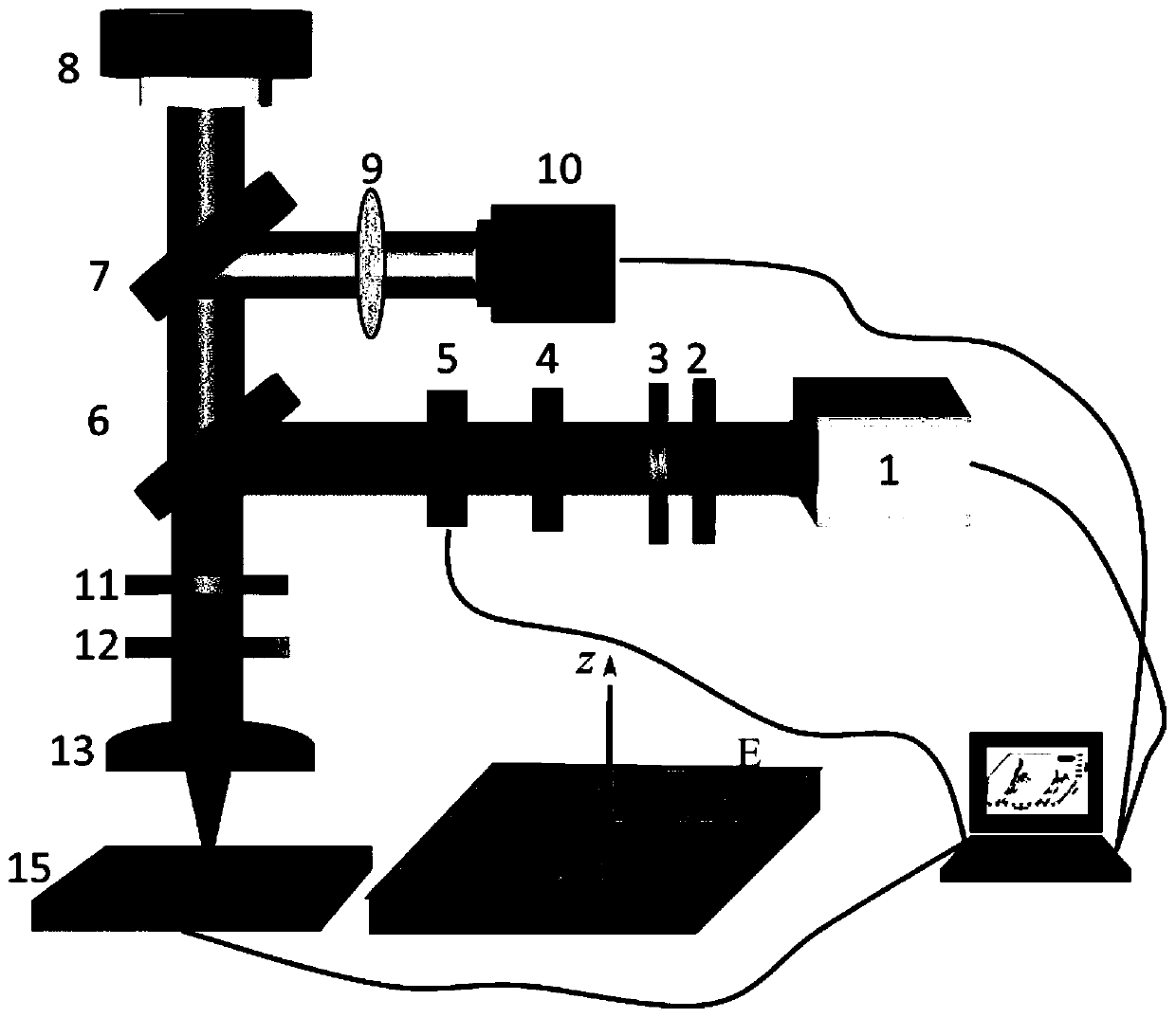
[0035] To process different forms of crystalline Ge 2 Sb 2 Te 5 Taking the all-dielectric composite nanostructure with anisotropic geometric form as an example, the multi-pulse femtosecond laser control method of the present invention is adopted, and the femtosecond laser pulses used are linearly polarized. The specific processing steps are as follows:

[0036] Adjust the optical path to ensure that the incident direction of the laser is perpendicular to the surface of the processed sample;

[0037] (1) Sample preparation: In this example, 50nm thick Ge was plated on a 10mm×10mm×1mm silicon dioxide sample by magnetron sputtering. 2 Sb 2 Te 5 membrane;

[0038] (2) Adjust energy: use the combination of the first half-wave plate 2 and the polarizer 3 and the neutral density attenuation plate 4 to adjust the laser energy to make it greater than the ablation threshold of 1.1 μJ on the surface of the processed sample film, and the laser energy can be continuously adjusted;

...

Embodiment 2

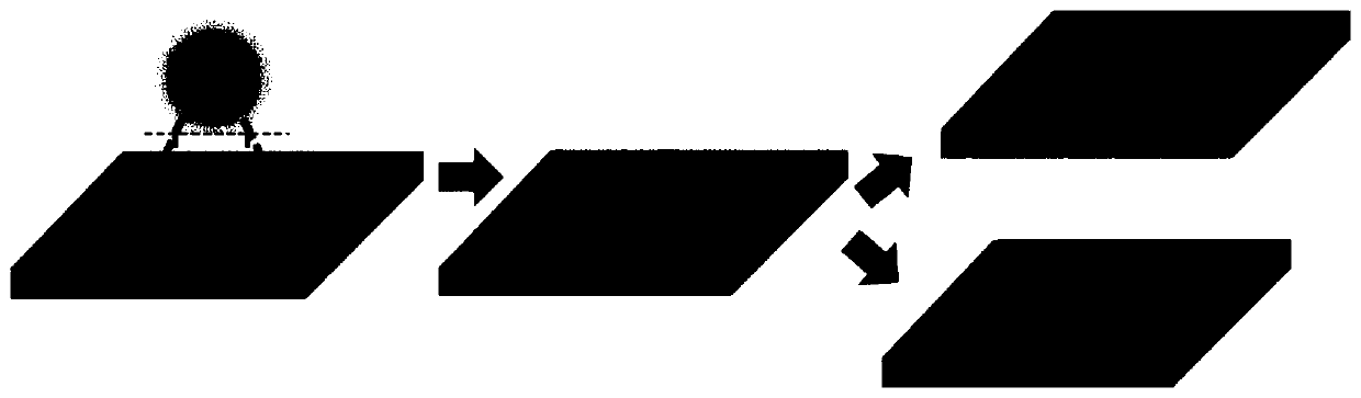
[0043] Preparation of crystalline Ge by eliminating linear polarization with multiple pulses 2 Sb 2 Te 5 The anisotropy of the composite nanostructure makes it present an isotropic geometric form as an example. Using the multi-pulse femtosecond laser processing polarization control method of the present invention, the femtosecond laser pulses used are circularly polarized. The specific processing steps are as follows:

[0044] Other steps are identical with embodiment 1, and difference is: before step (2) energy regulation is carried out, add quarter-wave plate 12 in optical path, adjust quarter-wave plate 12, make wave plate optical axis direction and The included angle of the original laser polarization direction is 45° to obtain circularly polarized femtosecond laser pulses.

[0045] In step (5), processing is performed under the condition of circularly polarized femtosecond laser pulses, and by changing the incident pulse energy, a uniformly arranged nanoparticle-single ...


PUM

PropertyMeasurementUnit
thicknessaaaaaaaaaa

Abstract

The invention discloses a method of controlling a geometric configuration of a GemSbnTek crystalline state nano structure by femtosecond laser regulation and control, and belongs to the field of femtosecond laser applications. According to the method, on the basis of preparing a multidimensional crystalline state nano structure by inducing a dewetting effect of an amorphous GemSbnTek thin-film material with a multiple-pulse femtosecond laser pulse, by controlling a polarization state of an incident femtosecond laser pulse, the control on the geometric configuration of the multidimensional nanostructure is realized. When adopting a linear polarization femtosecond laser pulse for irradiation, the obtained crystalline state nano structure is in an aeolotropic spindle-shaped geometric configuration, and the macro axis direction is perpendicular to the linear polarization direction of incident laser; and when adopting a circular polarization femtosecond laser pulse for the irradiation, theobtained crystalline state nano structure is in an isotropous spheroidal geometric configuration. The method is simple and effective; through the adjustment on the laser polarization state, the geometric configuration of the produced nano structure is accurately controlled, so that the optical response of a dielectric medium nano structure is controlled. The method has a vital application prospect in the aspect of optical control on large-area and low-loss photon applications.

Description

technical field [0001] The invention relates to the application field of femtosecond lasers, in particular to a method of controlling the multi-pulse induction of femtosecond lasers to induce amorphous Ge m Sb n Te k A method for the geometry regulation of crystalline nanostructures in the preparation of thin films. Background technique [0002] Once discovered, metamaterials have attracted widespread attention. It is generally believed that metamaterials are composite structures with physical properties that are not found in nature. At present, metamaterials are mostly arranged on the surface of the material in a repeated manner by structures smaller than the optical wavelength. Such structures can be materials such as metals and dielectrics. In recent years, metamaterial alternatives based on the surface plasmon resonance properties of noble metals have attracted extensive attention in the academic community to overcome the free-carrier absorption losses exhibited by no...

Claims


Application Information

Patent Timeline
Patent Type & Authority Patents(China)
IPC IPC(8): B23K26/362B23K26/60B23K26/0622B23K26/046
CPCB23K26/046B23K26/0624B23K26/361B23K26/60
Inventor 韩伟娜刘富荣袁艳萍
Owner BEIJING UNIV OF TECH
Why Eureka
Try Eureka