A method of controlling the growth of metal nanorods
A technology of metal nano and metal islands, applied in the direction of nanotechnology, metal material coating process, vacuum evaporation plating, etc., can solve the problems of single raw material, irregularity, and high purity of metal nanorods, and achieve controllable effects. The effect of uniform diameter size distribution and simple operation
- Summary
- Abstract
- Description
- Claims
- Application Information
AI Technical Summary
Problems solved by technology
Method used
Image
Examples
Embodiment 1
[0042] The simulation experiment based on the kinetic Monte Carlo model specifically includes the following steps:
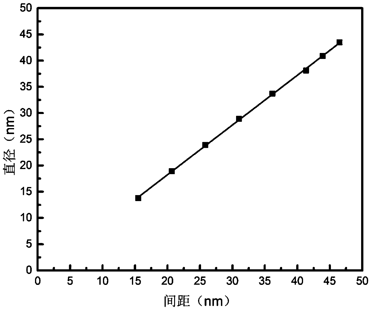
[0043] Step 1: Define a layer of substrate with a metal island array on the metal nanorod dynamics Monte Carlo model substrate according to the nanopatterning technology based on photolithography. The metal island array consists of several identical and uniformly distributed square Composed of metal islands, the size of the square metal islands is 3nm, and the distance between the metal islands is 15.5nm;
[0044] Step 2: Set the basic physical parameters of copper in the metal nanorod dynamics Monte Carlo model (the diffusion barrier is 0.06eV, the two-dimensional step barrier is 0.16eV, the three-dimensional step barrier is 0.40eV, and the vibration frequency pre-factor setting 5×10 12 s-1);
[0045] Step 3: Set the growth parameters in the metal nanorod dynamics Monte Carlo model: the temperature is 300K, the deposition rate is 8nm / s, the deposition inciden...
Embodiment 2
[0048] The simulation experiment based on the kinetic Monte Carlo model specifically includes the following steps:
[0049] Step 1: Define a layer of substrate with a metal island array on the metal nanorod dynamics Monte Carlo model substrate according to the nanopatterning technology based on photolithography. The metal island array consists of several identical and uniformly distributed square Composed of metal islands, the size of the square metal islands is 3nm, and the distance between the metal islands is 15.5nm;
[0050] Step 2: Set the basic physical parameters of copper in the metal nanorod dynamics Monte Carlo model (the diffusion barrier is 0.06eV, the two-dimensional step barrier is 0.16eV, the three-dimensional step barrier is 0.40eV, and the vibration frequency pre-factor setting 5×10 12 s-1);
[0051] Step 3: Set the growth parameters in the metal nanorod dynamics Monte Carlo model: the temperature is 300K, the deposition rate is 8nm / s, the deposition inciden...
Embodiment 3
[0054] The simulation experiment based on the kinetic Monte Carlo model specifically includes the following steps:
[0055] Step 1: Define a layer of substrate with a metal island array on the metal nanorod dynamics Monte Carlo model substrate according to the nanopatterning technology based on photolithography. The metal island array consists of several identical and uniformly distributed square Composed of metal islands, the size of the square metal islands is 3nm, and the distance between the metal islands is 15.5nm;
[0056] Step 2: Set the basic physical parameters of copper in the metal nanorod dynamics Monte Carlo model (the diffusion barrier is 0.06eV, the two-dimensional step barrier is 0.16eV, the three-dimensional step barrier is 0.40eV, and the vibration frequency pre-factor setting 5×10 12 s-1);
[0057] Step 3: Set the growth parameters in the metal nanorod dynamics Monte Carlo model: the temperature is 200K, the deposition rate is 8nm / s, the deposition inciden...
PUM
| Property | Measurement | Unit |
|---|---|---|
| diameter | aaaaa | aaaaa |
| diameter | aaaaa | aaaaa |
| angle | aaaaa | aaaaa |
Abstract
Description
Claims
Application Information


