Manufacturing method of array substrate, array substrate and display panel

A technology of an array substrate and a manufacturing method, applied in the display field, can solve the problem of high manufacturing difficulty of the array substrate, and achieve the effects of reducing the overall manufacturing difficulty, reducing the manufacturing difficulty, and avoiding poor electrical conductivity

Active Publication Date: 2018-07-17
BOE TECH GRP CO LTD
View PDF4 Cites 52 Cited by
  • Summary
  • Abstract
  • Description
  • Claims
  • Application Information

AI Technical Summary

Problems solved by technology

[0004] The present application provides a method for manufacturing an array substrate, an array substrate and a display panel, which can solve the problem that the overall manufacturing difficulty of the existing array substrate is relatively high

Method used


Image

  • Manufacturing method of array substrate, array substrate and display panel
  • Manufacturing method of array substrate, array substrate and display panel
  • Manufacturing method of array substrate, array substrate and display panel

Examples


Embodiment Construction

[0079] In order to make the object, technical solution and advantages of the present invention clearer, the implementation manner of the present invention will be further described in detail below in conjunction with the accompanying drawings.

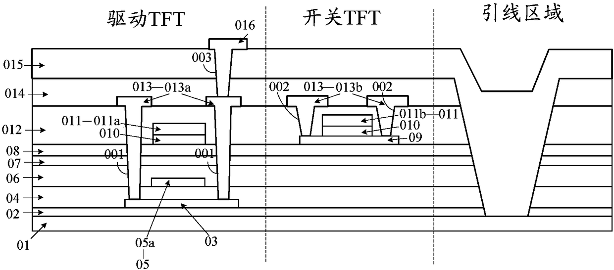
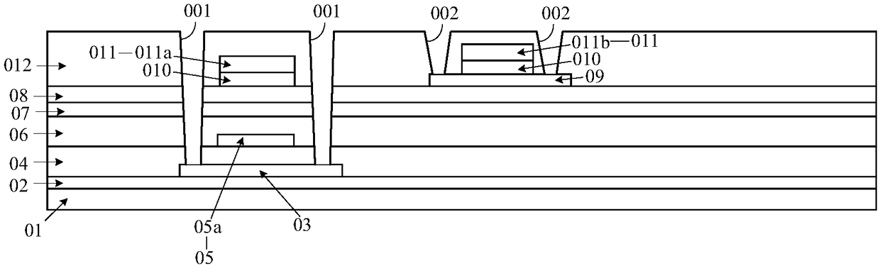
[0080] Please refer to Figure 1A , Figure 1A It is a schematic structural diagram of an array substrate in an AMOLED display provided in the related art. The array substrate may include: a base substrate 01, on which are sequentially arranged: a first buffer layer 02, a first active layer pattern 03 , the first gate insulating layer 04, the first gate pattern 05, the second gate insulating layer 06, the first interlayer dielectric layer 07, the second buffer layer 08, the second active layer pattern 09, the third gate An insulating layer 010, a second gate pattern 011, a second interlayer dielectric layer 012, a source-drain pattern 013, a passivation layer 014 and a planar layer pattern 015. Wherein, the first gate pattern 05 includ...


PUM


Abstract

The invention discloses a manufacturing method of an array substrate, the array substrate and a display panel and belongs to the technical field of display. The method comprises the steps as follows:a first thin film transistor and a second thin film transistor are formed on a substrate, wherein the first thin film transistor comprises a first active layer graph, a first gate, a first source anda first drain; the second thin film transistor comprises a second active layer graph, a second gate, a second source and a second drain; the first source, the first drain and the second gate are formed by adopting a primary composition process; and the second source and the second drain are formed by adopting the primary composition process. The first source, the first drain and the second gate are formed by adopting the primary composition process, and the second source and the second drain are formed by adopting the primary composition process, so that the overall manufacturing difficulty ofthe array substrate is reduced under the condition of not increasing the composition process.

Description

technical field [0001] The present invention relates to the field of display technology, in particular to a method for manufacturing an array substrate, an array substrate and a display panel. Background technique [0002] At present, an active matrix organic light emitting diode (English: Active-matrix organic light emitting diode; abbreviation: AMOLED) display is a new type of display on the market, and the pixel driving circuit in the AMOLED display usually includes two thin film transistors (English: Thin Film Transistor ; Abbreviation: TFT) and a storage capacitor, the two TFTs are respectively: a switching TFT (English: Switching TFT) and a driving TFT (English: Driving TFT). Both of the two TFTs may include: a gate, an active layer pattern and a source and a drain. [0003] When the scanning line is turned on, a certain voltage is applied to the gate of the switching TFT, and the current flows from the source of the switching TFT to the drain, and is transmitted to t...

Claims


Application Information

Patent Timeline
Patent Type & Authority Applications(China)
IPC IPC(8): H01L27/12H01L21/77H01L27/32
CPCH01L27/1214H01L27/1259H10K59/12H01L27/1225H01L27/1255H01L29/78633H10K59/1213H10K59/126H01L29/78618H01L29/78645H10K59/1216H10K59/1201
Inventor 卢鑫泓王珂胡合合宁策杨维
Owner BOE TECH GRP CO LTD
Why Eureka
Try Eureka