Silicon-based gan-based photonic chip and preparation method for blue-light visible light communication

A visible light communication and photonic chip technology, applied in the direction of optical waveguide light guide, optics, light guide, etc., to achieve high integration, small size, and increase the effect of information transmission rate

Active Publication Date: 2020-04-21
NANJING UNIV OF POSTS & TELECOMM
View PDF10 Cites 0 Cited by
  • Summary
  • Abstract
  • Description
  • Claims
  • Application Information

AI Technical Summary

Problems solved by technology

[0003] At present, another major bottleneck restricting the application of visible light wireless communication technology is the miniaturization and miniaturization of transceivers and signal processing modules.

Method used


Image

  • Silicon-based gan-based photonic chip and preparation method for blue-light visible light communication
  • Silicon-based gan-based photonic chip and preparation method for blue-light visible light communication
  • Silicon-based gan-based photonic chip and preparation method for blue-light visible light communication

Examples


Embodiment Construction

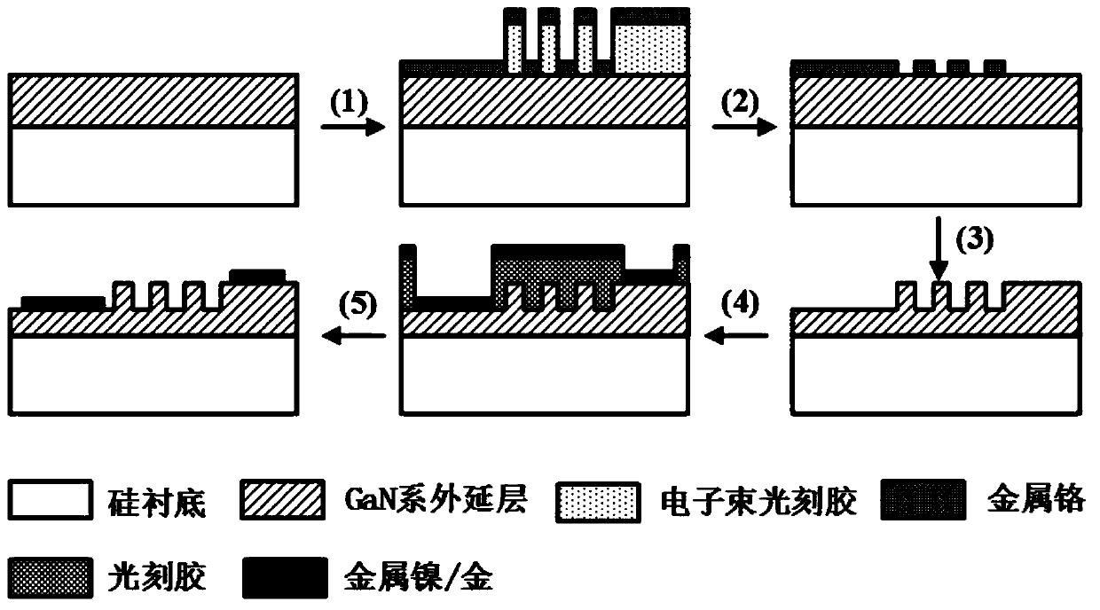
[0030] Below in conjunction with accompanying drawing, technical scheme of the present invention is described in further detail:

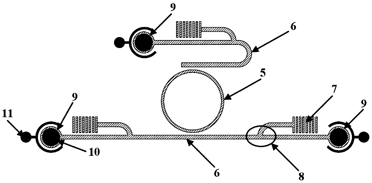
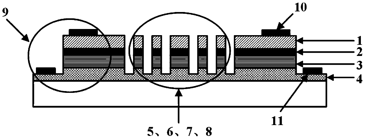
[0031] Such as figure 1 As shown, the silicon-based GaN-based photonic chip for blue light and visible light communication of the present invention realizes that the carrier is a silicon substrate nitride wafer, and the silicon substrate nitride wafer includes a top layer nitride with a low refractive index cladding layer and a The silicon substrate layer below the top nitride layer. A low-refractive-index cladding layer is arranged under the active layer of the top layer nitride of the silicon substrate nitride wafer, and an N-type GaN layer is arranged under the low-refractive index cladding layer; Active photonic devices that generate and receive blue light signals, LED blue light emitting devices and dual-function optoelectronic devices; silicon substrate nitride wafers with passive photonic devices for transmitting and processing blue light sig...


PUM


Abstract

The invention discloses a silicon-based GaN system photonic chip for blue light visible light communication and a preparation method thereof. A silicon-substrate nitride chip with a carrier of a low refractivity cladding is achieved, the silicon-substrate nitride chip comprises a silicon substrate layer and a top nitride with the low refractivity cladding located on the silicon substrate layer, and a nanometer optical waveguide, a shunt, a resonance loop, a coupling optical grating and a nickel / gold electrode used for power-on are arranged on the top nitride. The chip has the advantages of being small in size, has high integration and can be applied to the fields of optical computation, visible light communication and the like, and performance indexes of a blue light wavelength visible light communication technology in multiple aspects of information transmission speed, information processing speed, terminal component integration and the like are improved.

Description

technical field [0001] The invention relates to a silicon-based GaN-based photonic chip and a preparation method for blue-light visible light communication, and belongs to the technical field of information materials and devices. Background technique [0002] Visible light communication is a wireless optical communication technology developed based on LED devices. It utilizes its high-speed response characteristics of output optical power and driving current, and uses visible light as an information carrier to realize wireless communication. Visible light communication technology is green and low-carbon, can realize almost zero energy consumption communication, and can effectively avoid weaknesses such as radio communication electromagnetic signal leakage, and quickly build an anti-interference and anti-interception security information space. Within the spectrum of visible light, the blue light band has shorter wavelengths and a wider spectral band. [0003] At present, an...

Claims


Application Information

Patent Timeline
Patent Type & Authority Patents(China)
IPC IPC(8): G02B6/12
CPCG02B6/12007
Inventor 李欣王永进施政高绪敏朱刚毅
Owner NANJING UNIV OF POSTS & TELECOMM
Why Eureka
Try Eureka