Organic light-emitting display device and preparation method thereof

A light-emitting display and organic technology, applied in semiconductor/solid-state device manufacturing, electrical components, electric solid-state devices, etc., can solve problems such as low product reliability, poor product appearance, packaging impact, etc., achieve better packaging effect, shorten the drilling time Hole time, effects of avoiding impact

Active Publication Date: 2018-07-27
TRULY HUIZHOU SMART DISPLAY
View PDF3 Cites 4 Cited by
  • Summary
  • Abstract
  • Description
  • Claims
  • Application Information

AI Technical Summary

Problems solved by technology

Because there will be gas in the round hole area, when the laser is used to open the hole, due to the high energy and high temperature of the laser, the gas in the round hole will expand due to h

Method used


Image

  • Organic light-emitting display device and preparation method thereof
  • Organic light-emitting display device and preparation method thereof
  • Organic light-emitting display device and preparation method thereof

Examples


preparation example Construction

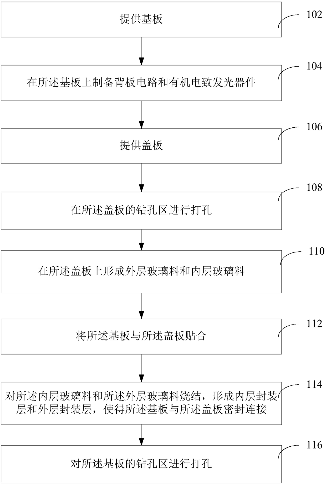
[0044] For example, a method for preparing an organic light-emitting display device includes: providing a substrate; preparing a backplane circuit and an organic electroluminescent device on the substrate; providing a cover plate; drilling holes in the drilling area of ​​the cover plate; Forming an outer layer of glass frit and an inner layer of glass frit on the cover plate; attaching the substrate to the cover plate; sintering the inner layer of glass frit and the outer layer of glass frit to form an inner encapsulation layer and an outer encapsulation layer, so that the substrate and the cover plate are hermetically connected; and drilling holes in the drilling area of ​​the substrate.

[0045] In the above embodiment, the cover plate is drilled before the base plate and the cover plate are bonded and packaged, so that the drilling process after the base plate and the cover plate are packaged is reduced, the drilling time of the base plate is effectively shortened, the drill...

Embodiment 1

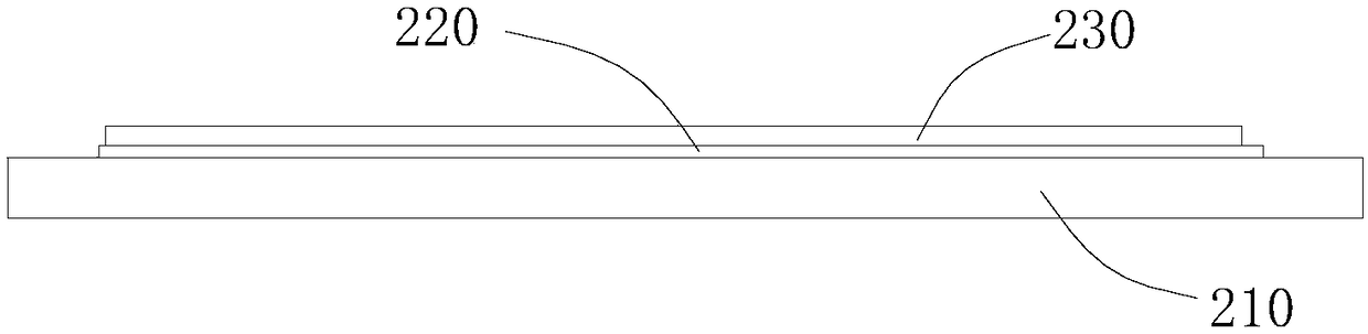
[0101] Step 1. Fabricate the backplane circuit and anode on the glass substrate according to the conventional LTPS process. Remove all the metal and photoresist at the punch hole and encapsulation layer. Subsequently, organic light-emitting and cathode and other functional layers are prepared, such as figure 2 .

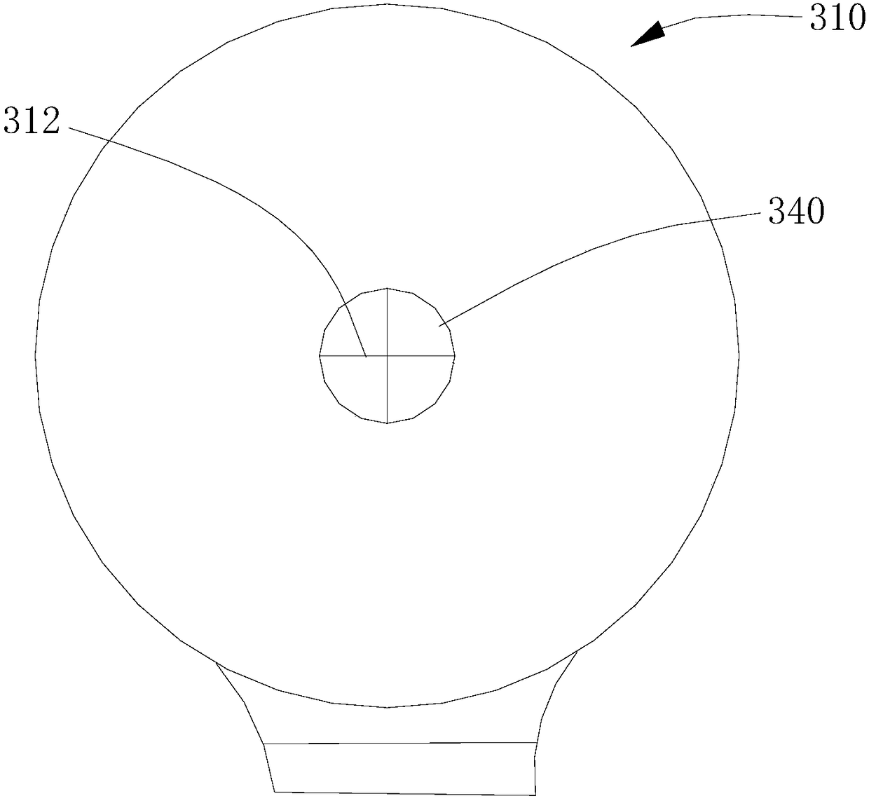
[0102] Step 2. Screen-print the coordinates of the hole on the cover, and mark the hole as the center of a circle or a "ten" or similar shape. Such as image 3 . The diameter of the opening is smaller than the diameter of the frit pattern of the inner ring.

[0103] Step 3: Use punching equipment to make holes on the cover plate according to the position of the hole mark.

[0104] Step 4. Silk-screen the Frit pattern on the cover, including the outer pattern Frit and the inner pattern Frit, such as Figure 4 .

[0105] Step 5: The base plate and the cover plate are bonded together, and the frit pattern of the inner ring is laser sintered first, and then the f...

Embodiment 2

[0108] Step 1. According to the conventional LTPS process, make the backplane circuit on the glass substrate and remove all the metal and photoresist at the position of the anode hole and the position of the packaging layer, and then prepare functional layers such as organic light emitting and cathode, such as figure 2 .

[0109] Step 2. Screen-print the coordinates of the opening on the cover plate. The opening is marked as a circle or a "ten", such as image 3 .

[0110] Step 3: Use punching equipment to make holes on the cover plate according to the position of the hole mark.

[0111] Step 4. Silk-screen the Frit pattern on the cover, including the outer pattern Frit and the inner pattern Frit, such as Figure 4 .

[0112] Step 5: The base plate and the cover plate are bonded together, and the frit pattern of the inner ring is laser sintered first, and then the frit pattern of the outer ring is sintered, such as Figure 5 .

[0113] Step 6: Opening holes on the substr...


PUM

PropertyMeasurementUnit
Thicknessaaaaaaaaaa
Thicknessaaaaaaaaaa

Abstract

The invention relates to an organic light-emitting display device and preparation method thereof. The method comprises the following steps: providing a substrate; preparing a backboard circuit and anorganic electroluminescent device on the substrate; providing a cover plate; drilling on a drilling area of the cover plate; forming outer frit and inner frit on the cover plate; fitting the substratewith the cover plate, sintering the outer frit and the inner frit, thereby enabling the substrate to hermetically connect with the cover plate; and drilling the drilling area of the substrate. The substrate is drilled before fitting and packaging the substrate and the cover plate, so that the drilling process is reduced after the substrate and the cover plate are packaged, thereby effectively shortening the drilling time on the substrate, reducing drilling heat quantity, and avoiding the influence on the packaged frit; the package effect is better, and the whole appearance of the organic light-emitting display device is better.

Description

technical field [0001] The invention relates to the technical field of organic light-emitting display manufacturing, in particular to an organic light-emitting display device and a preparation method thereof. Background technique [0002] OLED (Organic Light-Emitting Diode, organic light-emitting diode) display has the advantages of self-illumination, ultra-thin, fast response, wide viewing angle, low power consumption, etc., and is considered to be the most potential display device. AMOLED (Active-matrix organic light emitting diode, active matrix organic electroluminescent device) can give full play to OLED (Organic Light-Emitting Diode, organic light-emitting diode) process is simple, high luminous efficiency, light and thin, rich colors and wide viewing angle, etc. Advantages, it can be used in large-size displays, and it can also play a potential role in micro-displays. [0003] With the wide application of AMOLED, AMOLED screen needs to meet the screen design requirem...

Claims


Application Information

Patent Timeline
IPC IPC(8): H01L51/52H01L27/32
CPCH10K59/12H10K50/841
Inventor 柯贤军张雪峰王萃梓苏君海李建华
Owner TRULY HUIZHOU SMART DISPLAY
Why Eureka
Try Eureka