Vacuum heating system, and wafer stripping device and method

A vacuum heating and peeling device technology, which is applied in metal processing equipment, manufacturing tools, laser welding equipment, etc., can solve the problem that the wafer and the substrate cannot be completely separated, and achieve the effects of avoiding damage, facilitating handling, and improving yield

Active Publication Date: 2018-07-31
深圳市大族半导体装备科技有限公司
View PDF6 Cites 1 Cited by
  • Summary
  • Abstract
  • Description
  • Claims
  • Application Information

AI Technical Summary

Problems solved by technology

[0006] In view of the above-mentioned deficiencies in the prior art, the object of the present invention is to provide a vacuum heating system, a wafer peeling device and method, thereby overcoming the problem that the wafer and the substrate cannot be completely separated in the wafer peeling method in the prior art

Method used


Image

  • Vacuum heating system, and wafer stripping device and method
  • Vacuum heating system, and wafer stripping device and method
  • Vacuum heating system, and wafer stripping device and method

Examples


Embodiment Construction

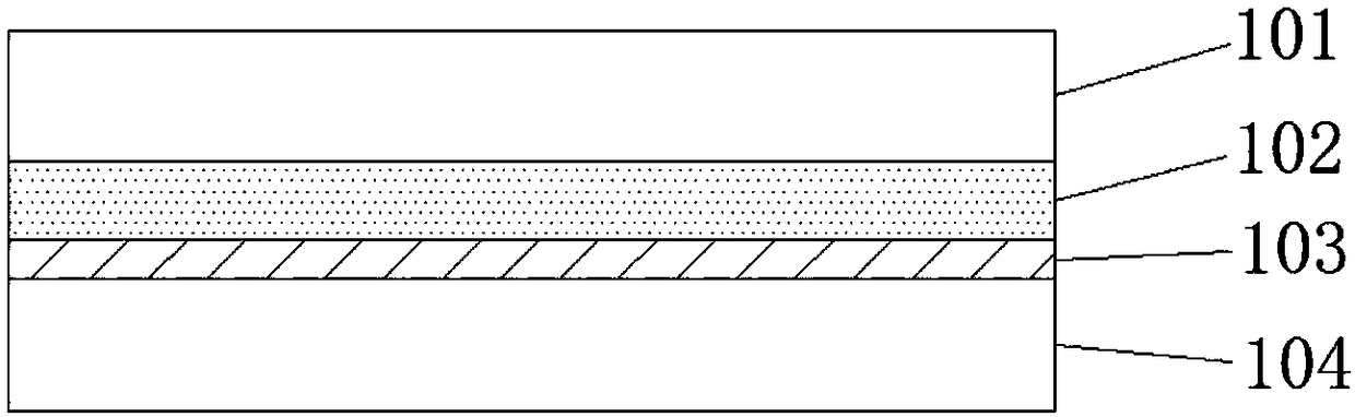
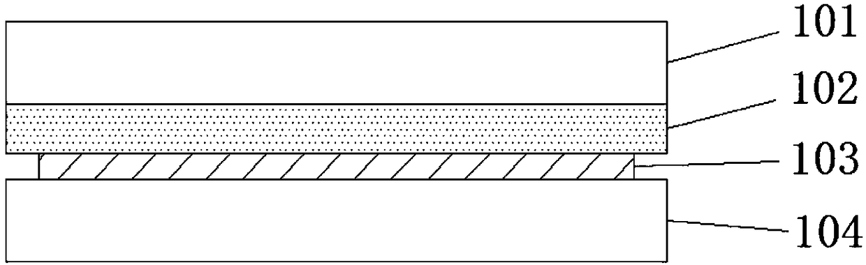
[0045] The present invention provides a vacuum heating system, wafer peeling device and method. In order to make the purpose, technical solution and effect of the present invention clearer and clearer, the present invention will be further described in detail below with reference to the accompanying drawings and examples. It should be understood that the specific embodiments described here are only used to explain the present invention, not to limit the present invention.

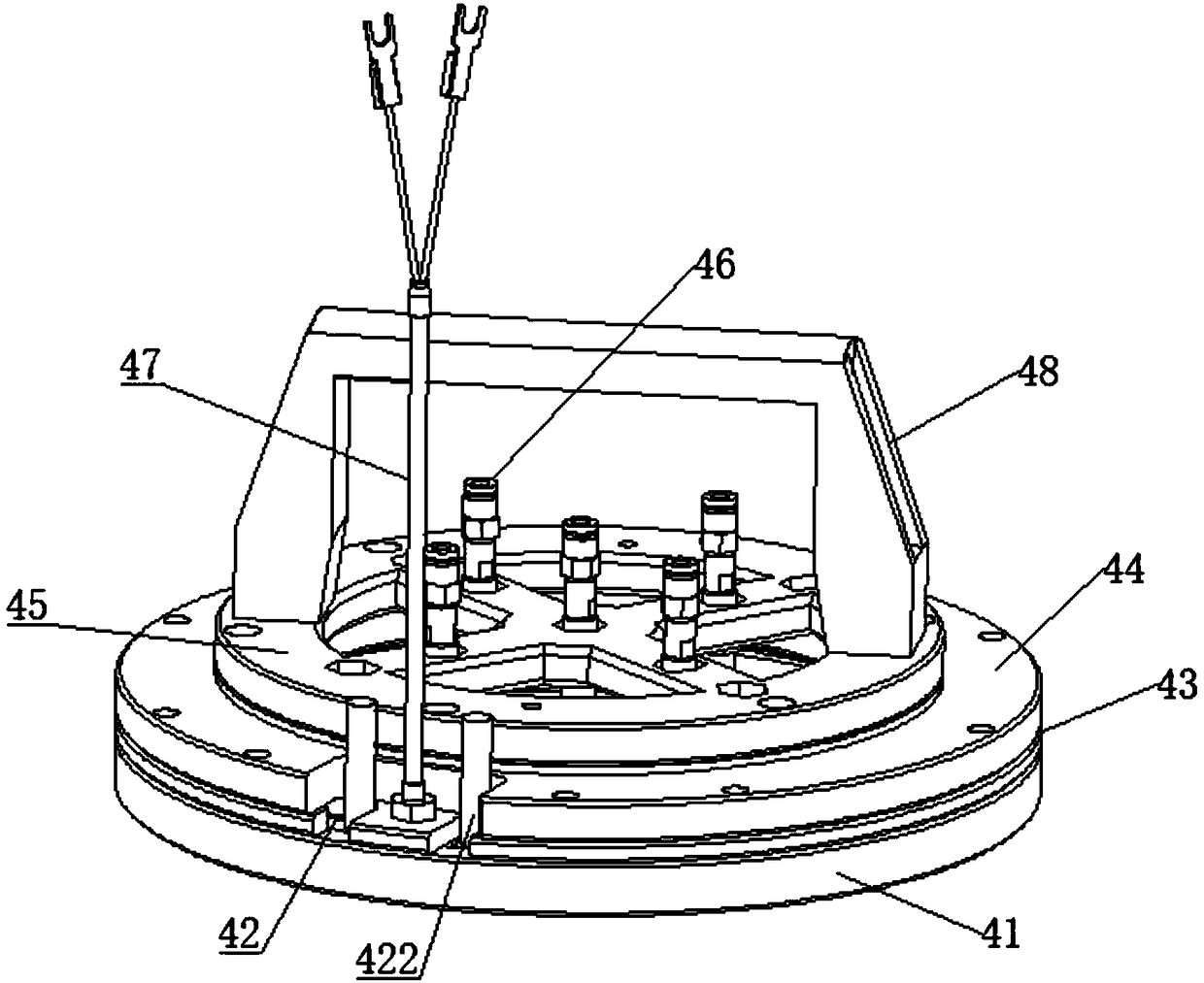
[0046] The wafer stripping device of the embodiment of the present invention, such as image 3 As shown, the vacuum heating system 4 includes: heating ring fixing plate 41, heating ring 42, heating ring cover plate 43, heat insulation plate 44, suction nozzle fixing plate 45, vacuum suction nozzle 46, temperature sensor 47 (thermocouple) .

[0047] Further, in this embodiment, as image 3 , Figure 4 As shown, the heating ring fixing plate 41 is ring-shaped, and has a ring-shaped groove 411, which is mad...


PUM

PropertyMeasurementUnit
thicknessaaaaaaaaaa
depthaaaaaaaaaa
thicknessaaaaaaaaaa

Abstract

The invention discloses a vacuum heating system, and a wafer stripping device and method. The vacuum heating system comprises a heating ring fixing plate, a heating ring, a thermal insulation plate, asuction nozzle fixing plate and a plurality of vacuum suction nozzles, wherein the heating ring fixing plate is in an annular shape and is provided with a circle of annular groove; the heating ring is in the annular shape and is arranged in the groove of the heating ring fixing plate; the thermal insulation plate is in the annular shape and is arranged above the heating ring; the suction nozzle fixing plate is arranged above the thermal insulation plate; and the plurality of vacuum suction nozzles are symmetrically and uniformly arranged on the suction nozzle fixing plate and are used for adsorbing a stripped wafer and removing the wafer. In the invention, through arranging the vacuum heating system, a bonding layer material can be heated in an area where the wafer is bonded and can be melted so that the wafer is completely stripped. Simultaneously, through the vacuum suction nozzles of the vacuum heating system, the stripped wafer can be adsorbed so that the wafer is convenient to carry, the wafer is prevented from be damaged and the yield rate of wafer stripping is increased.

Description

technical field [0001] The invention relates to the technical field of semiconductor processing, in particular to a vacuum heating system, a wafer stripping device and a method. Background technique [0002] Integrated circuit packaging is one of the core links in the semiconductor industry chain. In recent years, stacked chip packaging has gradually become the mainstream of technological development. Stacked chip packaging technology, referred to as 3D packaging, refers to the packaging technology that stacks more than two chips in the same package in the vertical direction without changing the size of the package. It originated from the flash memory (NOR / NAND ) and stacked packaging of SDRAM. [0003] With the increasing demand for large-scale integration and high-density packaging, the thickness of each layer of chips used in the stack will inevitably need to be thinned. At present, the chip thickness of more advanced stacked packages is below 100um. For some application...

Claims


Application Information

Patent Timeline
Patent Type & Authority Applications(China)
IPC IPC(8): H01L21/67H01L21/683B23K26/064B23K26/18
CPCB23K26/18B23K26/064H01L21/67103H01L21/6838
Inventor 冯玙璠陈治贤庄昌辉范小贞赵前来黄汉杰何江玲尹建刚高云峰
Owner 深圳市大族半导体装备科技有限公司
Why Eureka
Try Eureka