Micro-chip transfer printing device and system

A microchip and transfer printing technology, which is applied in transportation and packaging, electrical components, semiconductor/solid-state device manufacturing, etc., can solve the problems of low transfer printing rate, low production efficiency, and inability to cope with ultra-thin and small sizes, and achieve The effect of improving work efficiency, avoiding complicated operations, and reducing transfer costs

Active Publication Date: 2018-07-31
BOE TECH GRP CO LTD
View PDF4 Cites 19 Cited by
  • Summary
  • Abstract
  • Description
  • Claims
  • Application Information

AI Technical Summary

Problems solved by technology

Specifically, the principle of single-chip transfer printing equipment is: use the indenter to directly press the microchip from the stretch film to the circuit board. However, this method cannot correspond to ultra-thin and small sizes, and the transfer rate is low and the production efficiency is low. Low; the principle of batch transfer printing technology is: transfer in batches through intermolecular force or magnetic force, but the graphics transferred by this transfer printing method can only be transferred according to the surface graphics of the transfer head, and the patterned transfer cannot be flexibly realized. print

Method used


Image

  • Micro-chip transfer printing device and system
  • Micro-chip transfer printing device and system
  • Micro-chip transfer printing device and system

Examples


Embodiment Construction

[0031] The following will clearly and completely describe the technical solutions in the embodiments of the present invention with reference to the accompanying drawings in the embodiments of the present invention. Obviously, the described embodiments are only some, not all, embodiments of the present invention. Based on the embodiments of the present invention, all other embodiments obtained by persons of ordinary skill in the art without making creative efforts belong to the protection scope of the present invention.

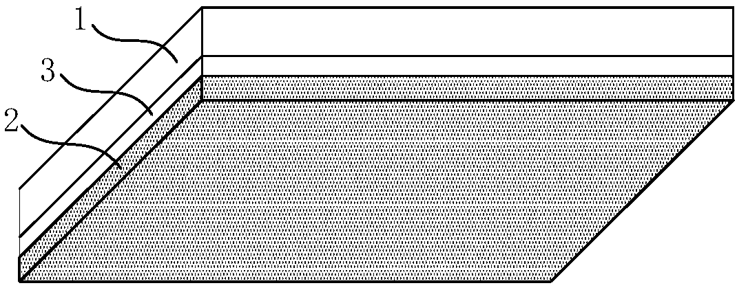
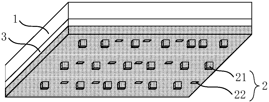
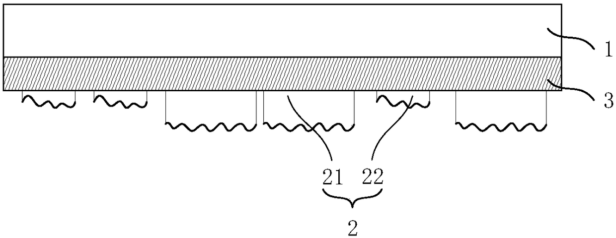
[0032] Please refer to Figure 1 to Figure 4 , the invention provides a microchip transfer device, comprising:

[0033] Indenter substrate 1;

[0034] The transfer array layer 2 provided on the side of the indenter substrate 1 facing the carrier substrate 4 and used to transfer the micro devices 5 on the carrier substrate 4, the transfer array layer 2 includes a number of transfer blocks distributed in an array on the indenter substrate 1 , each transfer blo...


PUM


Abstract

The invention relates to the technical field of transfer printing, and discloses a micro-chip transfer printing device and system. The device comprises a press head substrate; a transfer printing array layer which is disposed at one side, facing a bearing substrate, of the press head substrate, is used for the transfer printing of a miniature device on the bearing substrate, and comprises a plurality of transfer printing blocks distributed on the press head substrate in an array, wherein each transfer printing block has a non-pick-up state and a pick-up state for picking up the miniature device, and the switching of each transfer printing block between the non-pick-up state and the pick-up state is independently controllable. The switching of each transfer printing block the device betweenthe non-pick-up state and the pick-up state is independently controllable. The device can achieve the patterning of the transfer printing array layer, achieves the simultaneous transfer printing of alarge number of miniature devices, also can change the patterns of the transfer printing array layer according to different transfer printing requirements, achieves the application of the transfer printing array layer under different transfer printing demands, avoids the complex replacement operation of a transfer printing head, and reduces the transfer printing cost of the miniature devices.

Description

technical field [0001] The invention relates to the technical field of transfer printing, in particular to a microchip transfer printing device and a microchip transfer system. Background technique [0002] A microchip is an integrated circuit chip made of microelectronics technology. It has developed into the Gigabit (core GSI) era. Portable supercomputers, electronic notebooks, miniature translators and portable phones made of microchips have gradually become popular. Appear. [0003] With the birth of the micro-pitch LED display, the micro-pitch LED display has been more and more used in Command center hall, control room, conference center and other key places. With the continuous shrinking of the pixel pitch of the micro-pitch LED display, people's viewing distance is further shortened. [0004] However, regardless of microchips, microsensors, microLEDs and other devices, the transfer and packaging of small-sized chips are still difficult, especially the technology fo...

Claims


Application Information

Patent Timeline
Patent Type & Authority Applications(China)
IPC IPC(8): H01L21/677
CPCH01L21/67706H01L21/67721
Inventor 陈小川梁蓬霞
Owner BOE TECH GRP CO LTD
Why Eureka
Try Eureka