

Composite patterned substrate using low-refractive index material as medium and manufacturing method thereof
A low-refractive index, graphics substrate technology, applied in the direction of electrical components, circuits, semiconductor devices, etc., can solve problems such as difficulties, and achieve the effects of saving growth time, increasing output rate, and improving light extraction efficiency
- Summary
- Abstract
- Description
- Claims
- Application Information
AI Technical Summary
Problems solved by technology
Method used
Image

Examples
Embodiment Construction
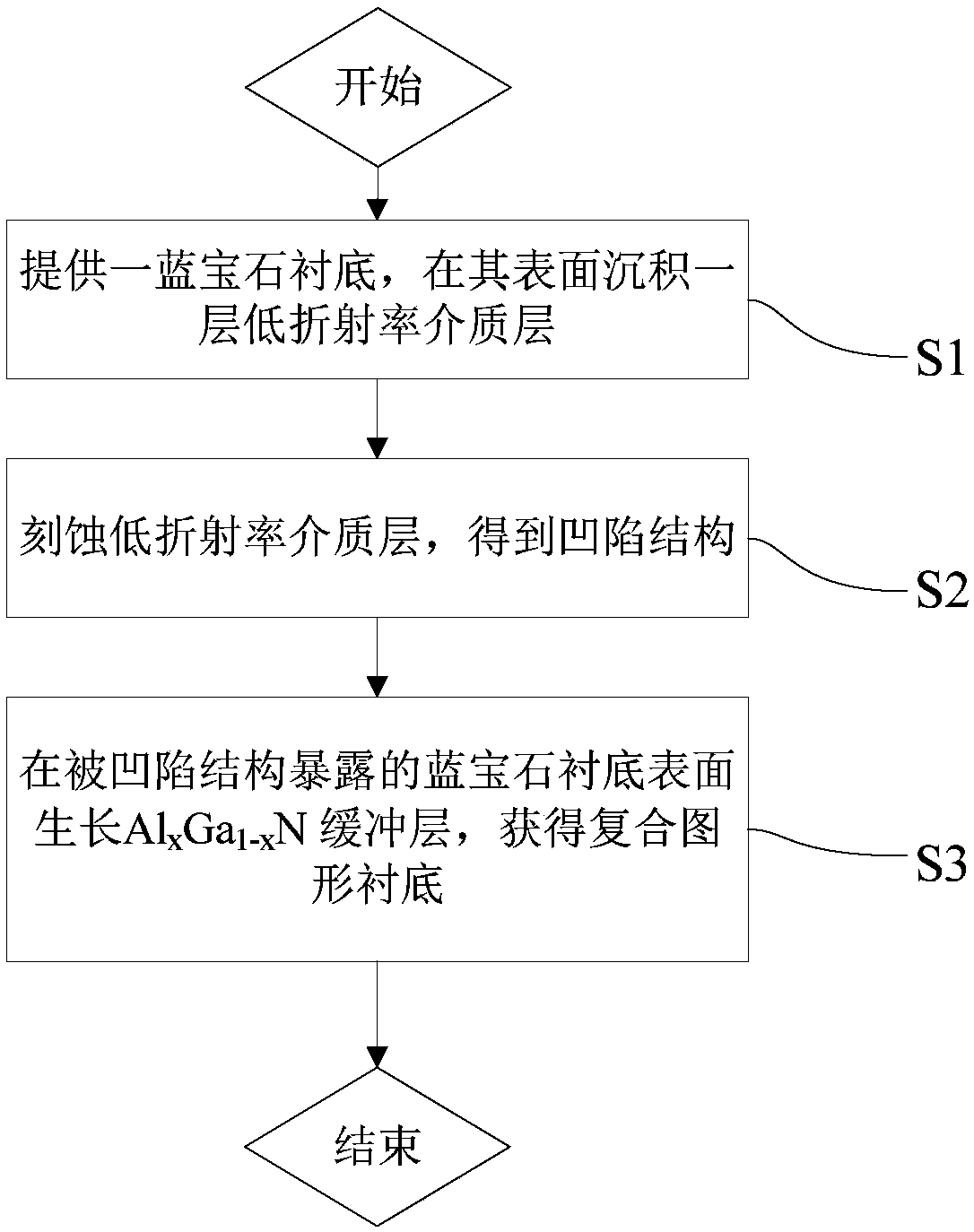
[0037] Embodiments of the present invention are described below through specific examples, and those skilled in the art can easily understand other advantages and effects of the present invention from the content disclosed in this specification. The present invention can also be implemented or applied through other different specific implementation modes, and various modifications or changes can be made to the details in this specification based on different viewpoints and applications without departing from the spirit of the present invention.
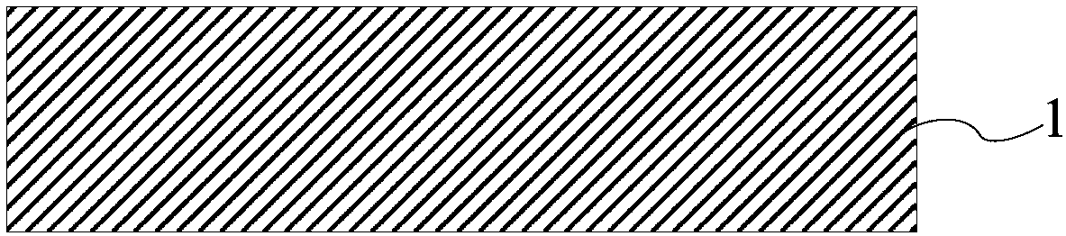
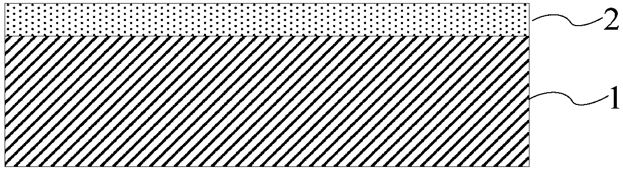
[0038] see Figure 1 to Figure 6 , It should be noted that the diagrams provided in this embodiment are only schematically illustrating the basic idea of the present invention, and only the components related to the present invention are shown in the diagrams rather than the number and shape of components in actual implementation. and size drawing, the type, quantity and proportion of each component can be changed arbitrarily during a...
PUM
| Property | Measurement | Unit |
|---|---|---|
| thickness | aaaaa | aaaaa |
| area | aaaaa | aaaaa |
| thickness | aaaaa | aaaaa |
Abstract
Description
Claims
Application Information