Compound, luminescent material and device, and display device

A technology of luminescent materials and compounds, which is applied in the fields of compounds, display devices, luminescent materials and devices, and can solve the problems of phosphorescent material efficiency roll-off, high production cost, and poor stability of phosphorescent devices, etc.

Active Publication Date: 2021-06-18
WUHAN TIANMA MICRO ELECTRONICS CO LTD +1
View PDF5 Cites 0 Cited by
  • Summary
  • Abstract
  • Description
  • Claims
  • Application Information

AI Technical Summary

Problems solved by technology

However, phosphorescent materials are basically heavy metal complexes such as Ir, Pt, Os, Re, Ru, etc., and the production cost is high, which is not conducive to large-scale production; and at high current densities, phosphorescent materials have a serious efficiency roll-off phenomenon; in addition, The stability of phosphorescent devices is also not good

Method used


Image

  • Compound, luminescent material and device, and display device
  • Compound, luminescent material and device, and display device
  • Compound, luminescent material and device, and display device

Examples


preparation example Construction

[0176] According to another aspect of the present invention, there is provided a preparation method of the compound as described above, comprising the following steps:

[0177] The activated benzocycloalkane group is reacted with the activated D unit and A unit respectively to obtain the compound.

[0178] Taking the preparation of compounds P1-P6, P19 and P21 as examples, the preparation method of the compound of the present invention will be described below.

[0179] Synthesis of Compound P1

[0180]

[0181] Weigh S1 (30mmol) into a 250mL two-necked flask, add 80mL of acetonitrile to dissolve S1, add dropwise an aqueous solution of HCl (volume ratio: 15mL:50mL), cool the reaction mixture to 0°C, and add the above mixture to NaNO 2 In an aqueous solution (35mmol:50mL), the reaction was carried out at a temperature lower than 5°C for 30min. The above reaction mixture solution was added to KI aqueous solution (44mmol:50mL). After the addition was completed, the reaction m...

Embodiment 1~8

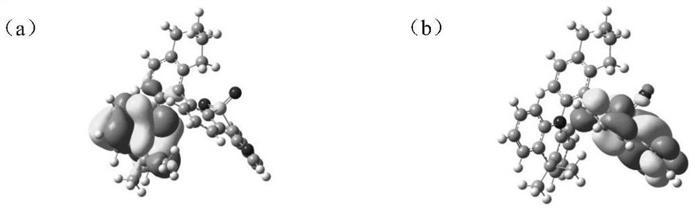
[0306] figure 1 Shows the orbital arrangement of compound P1, where, figure 1 (a) is the HOMO energy level distribution diagram of compound P1, figure 1 (b) is the LUMO energy level distribution diagram of compound P1. From figure 1 It can be clearly seen that the HOMO and LUMO of compound P1 are arranged on different units, achieving complete separation, which helps to reduce the intersystem energy difference ΔE ST , so as to improve the reverse intersystem crossing ability.

[0307] Using density functional theory (DFT), for compounds P1-P6, P19, P21, using the Gaussian 09 program package at the calculation level of B3LYP / 6-31G(d), the distribution of molecular frontier orbitals was optimized and calculated; at the same time Based on time-dependent density functional theory (TDDFT), the lowest singlet energy level S1 and the lowest triplet energy level T1 of the molecule were calculated by simulation.

[0308] The relevant data of Examples 1-8 are shown in Table 1. It ...


PUM


Abstract

The invention relates to the technical field of organic electroluminescent materials, in particular to a compound, a luminescent material, a device, and a display device. The compound has the structure shown below: the compound can be used as a thermally activated delayed fluorescence (TADF) material. The compound is used as a light-emitting material or a host material of a light-emitting layer of an organic electroluminescence device, and can realize higher light-emitting efficiency.

Description

technical field [0001] The invention relates to the technical field of organic electroluminescent materials, in particular to a compound, a luminescent material, a device, and a display device. Background technique [0002] According to the light-emitting mechanism, there are mainly four kinds of materials that can be used for the light-emitting layer of OLEDs: fluorescent materials, phosphorescent materials, triplet-triplet annihilation (TTA) materials, and thermally activated delayed fluorescence (TADF) materials. Among them, the theoretical maximum internal quantum yield of fluorescent materials does not exceed 25%, the theoretical maximum internal quantum yield of TTA materials does not exceed 62.5%; the theoretical maximum internal quantum yield of phosphorescent materials and TADF materials can reach 100%. However, phosphorescent materials are basically heavy metal complexes such as Ir, Pt, Os, Re, Ru, etc., and the production cost is high, which is not conducive to la...

Claims


Application Information

Patent Timeline
Patent Type & Authority Patents(China)
IPC IPC(8): C07D413/10C07D409/10C07D209/86C07F5/02C07D401/14C07D209/88C07D265/38C07D403/14C07D417/14C07D235/02C07D487/16C07D513/14C07D241/38C07F7/08C07D519/00C07D401/10C09K11/06H01L51/50H01L51/54
CPCC09K11/06C07D209/86C07D209/88C07D235/02C07D241/38C07D265/38C07D401/10C07D401/14C07D403/14C07D409/10C07D413/10C07D417/14C07D487/16C07D513/14C07D519/00C07F5/02C07F7/0807C09K2211/1096C09K2211/1088C09K2211/1092C09K2211/1029C09K2211/1014C09K2211/1007C09K2211/1011C09K2211/1059C09K2211/1051C09K2211/104C09K2211/1044C09K2211/1033C09K2211/1037H10K85/636H10K85/633H10K85/631H10K85/654H10K85/6576H10K85/6574H10K85/6572H10K85/657H10K85/40H10K50/11
Inventor 高威王湘成张磊牛晶华
Owner WUHAN TIANMA MICRO ELECTRONICS CO LTD
Why Eureka
Try Eureka