Infrared optical material microdefect detection device and far infrared microscope lens

An infrared optical material and micro-defect technology, which is applied in the directions of optical testing of flaws/defects, material analysis by optical means, measurement devices, etc., which can solve the problems of inability to observe and judge the use requirements of materials, and achieve more flexible detection positions. Change, detection more flexible, easy maintenance effect

Pending Publication Date: 2018-08-07
NINGBO SUNNY INFRARED TECH COMPANY
View PDF0 Cites 6 Cited by
  • Summary
  • Abstract
  • Description
  • Claims
  • Application Information

AI Technical Summary

Problems solved by technology

[0003] However, for infrared-transmitting optical materials, such as single crystal germanium and single crystal silicon, ordinary optical microscopes cannot observe the internal micro-defects of such materials due to their impermeability to visible light, making it impossible to judge whether the quality of the material meets the requirements for use.

Method used


Image

  • Infrared optical material microdefect detection device and far infrared microscope lens
  • Infrared optical material microdefect detection device and far infrared microscope lens

Examples


Embodiment Construction

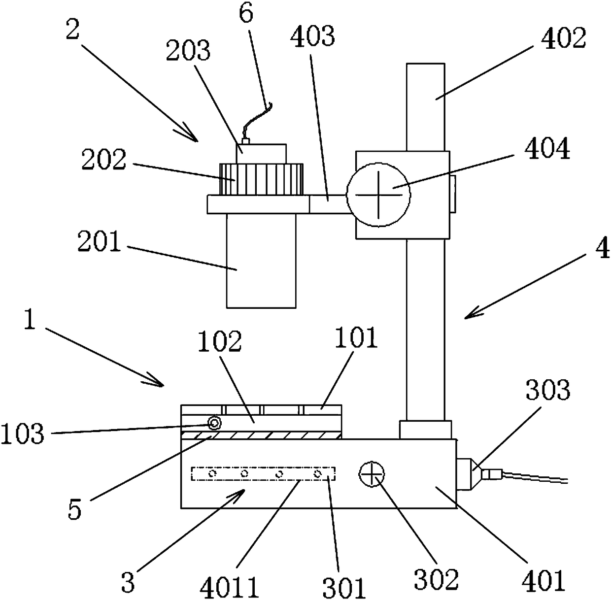
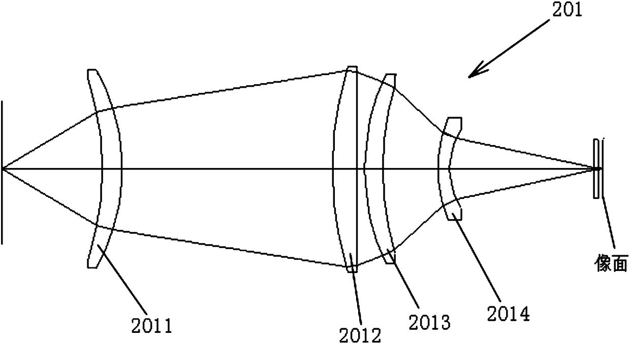
[0038] In order to more clearly describe the embodiments of the present invention or the technical solutions in the prior art, the following will briefly introduce the drawings that are used in the embodiments. Apparently, the drawings in the following description are only some embodiments of the present invention, and those skilled in the art can also obtain other drawings according to these drawings without creative efforts.

[0039] When describing the embodiments of the present invention, the terms "vertical", "transverse", "upper", "lower", "front", "rear", "left", "right", "vertical", " The orientation or positional relationship expressed by "horizontal", "top", "bottom", "inner" and "outer" is based on the orientation or positional relationship shown in the relevant drawings, which are only for the convenience of describing the present invention and simplifying the description, and It is not to indicate or imply that the device or element referred to must have a particu...


PUM


Abstract

The invention relates to an infrared optical material microdefect detection device, a far infrared microscope lens applied to the device, and a detection method of the detection device. The far infrared microscope lens comprises a first lens, a second lens, a third lens and a fourth lens sequentially arranged along an optical axis from an object side to an image side; the first lens, the third lens and the fourth lens are made of germanium glass; the second lens is made of chalcogenide glass; object side surfaces of the first lens and the third lens are spherical surfaces; image side surfacesof the first lens and the third lens are aspheric surfaces; the aspheric surface of the third lens is provided with a diffraction ring zone; the object side surfaces and the image side surfaces of thesecond lens and the fourth lens are spherical surfaces. The far infrared microscope lens provided by the invention can be used for observing microdefects far-infrared transmitted and unobserved by naked eyes inside infrared optical materials (silicon, germanium or chalcogenide glass and the like), so that different types of defects such as air bubbles, impurities and / or cracks can be clearly observed.

Description

technical field [0001] The invention relates to an infrared optical material microscopic defect detection device, a far-infrared microscope lens used in the device and a detection method of the detection device. The infrared rays emitted by the infrared light source pass through the infrared optical material to be tested, and the transmitted infrared rays are enlarged and imaged by the infrared microscope lens. The infrared detector converts the received infrared imaging signal into an electronic signal and then converts it into a graphic through a computer, so as to realize the inside of the material. Observe microscopic defects. Background technique [0002] An optical microscope uses one or a group of lenses to form an optical magnification system to magnify microscopic objects or images into images that can be resolved by the naked eye for people to observe the microscopic world. Optical microscopes generally use visible light as the light source. Most of the working me...

Claims


Application Information

Patent Timeline
Patent Type & Authority Applications(China)
IPC IPC(8): G01N21/88
CPCG01N21/8851G01N2021/8887
Inventor 周刚潘养辉朱光春陈惠广
Owner NINGBO SUNNY INFRARED TECH COMPANY
Why Eureka
Try Eureka