Fingerprint recognition chip device

A fingerprint identification and chip technology, which is applied in the direction of electrical components, electrical solid devices, circuits, etc., can solve problems such as poor electrical connection, poor electrical connection of welding wires, unfavorable protection of sensitive chips, etc., and achieve the effect of preventing lateral flow and reducing load

Active Publication Date: 2018-08-17
合肥源康信息科技有限公司
View PDF8 Cites 8 Cited by
  • Summary
  • Abstract
  • Description
  • Claims
  • Application Information

AI Technical Summary

Problems solved by technology

[0002] Existing fingerprint identification chip packaging mostly adopts a planar packaging process on the substrate, which is not conducive to the protection of sensitive chips when there are other sensitive chips; even some processes use stacked packaging, which uses support The fingerprint identification chip is loaded, but since the fingerprint identification chip needs to be adhered with adhesive resin, the excess resin will flow to the substrate, thereby covering the pads on the substrate, resulting in poor electrical connection of subsequent welding wires; And the solder soldered by the excess support will also flow to the substrate, resulting in the same disadvantage of poor electrical connection

Method used


Image

  • Fingerprint recognition chip device
  • Fingerprint recognition chip device
  • Fingerprint recognition chip device

Examples


no. 1 example

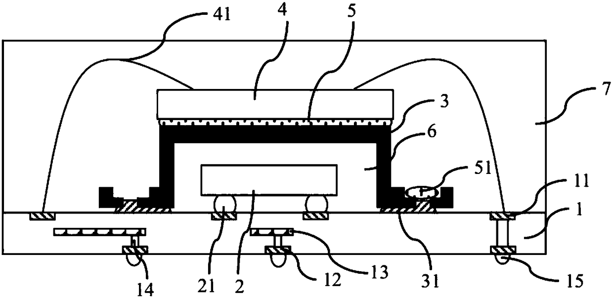
[0038] see Figure 1-2 , the fingerprint recognition chip device of the present invention, it comprises:

[0039] The redistribution substrate 1 has an opposite upper surface and a lower surface, a first pad 11 is arranged on the upper surface, a second pad 12 is provided on the lower surface, and the first pad 11 is connected to the first pad 12. The two pads 12 are electrically connected through the wiring layer 13 and / or the first through hole 14 in the redistribution substrate 1;

[0040] The first chip 2 is flip-chip-bonded on the redistribution substrate 1 through first solder balls 21, and is electrically connected to a part of the first pad 11;

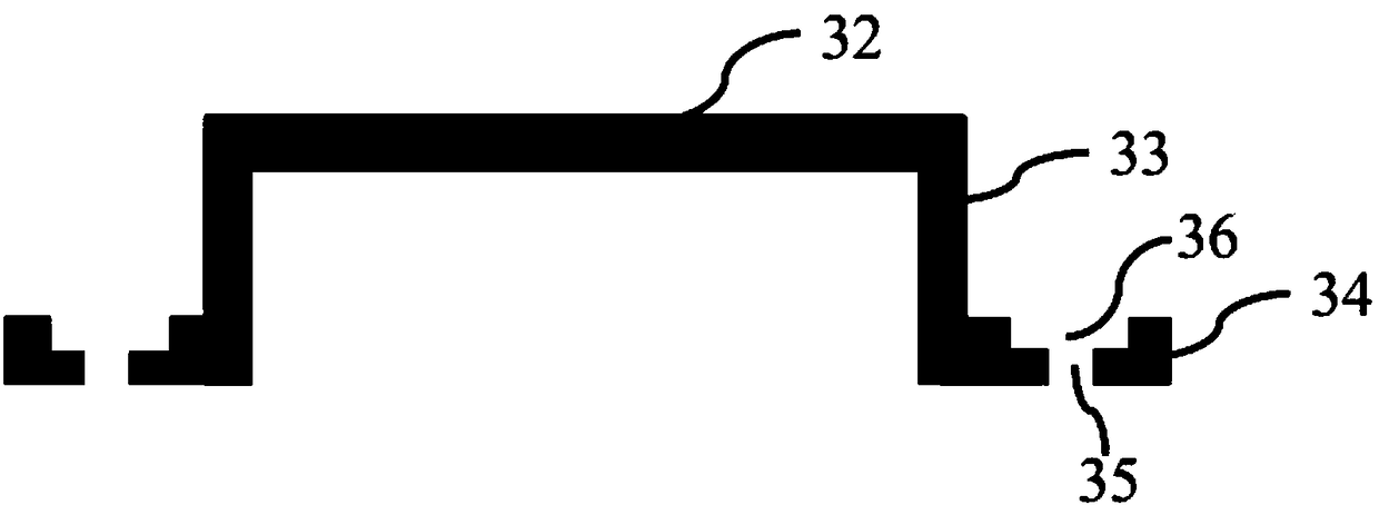
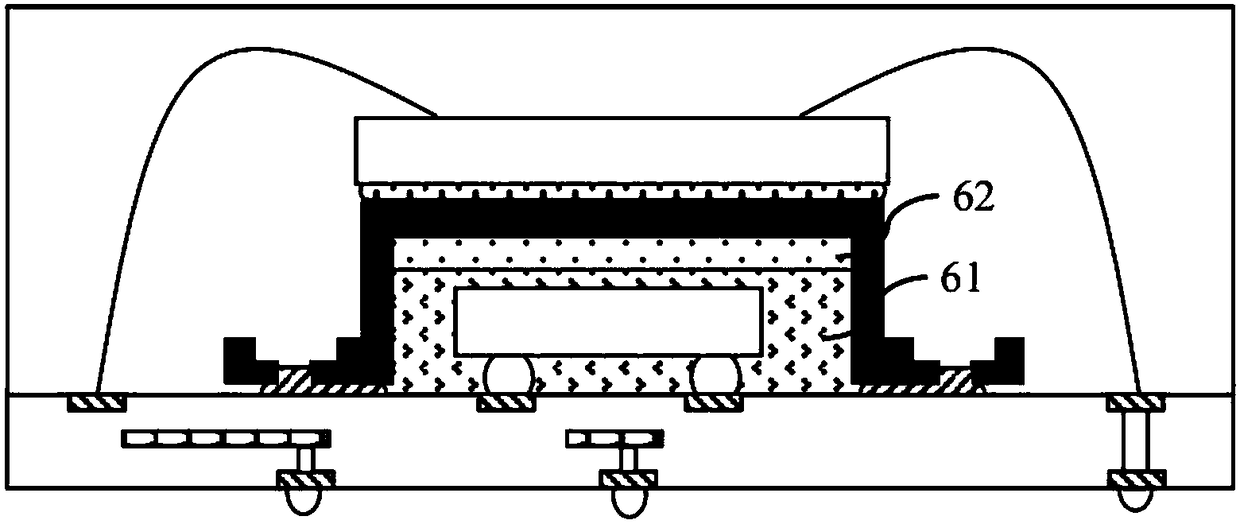
[0041] The support cover 3 is welded on the upper surface of the redistribution substrate 1 by solder 31, and forms a closed space 6 with the redistribution substrate 1, and the first chip 2 is located in the closed space 6;

[0042] The second chip 4 is a fingerprint identification chip, which is fixed on the top surface of...

no. 2 example

[0048] In the first embodiment, when pressure is applied to the upper surface of the second chip, it will cause pressure on both sides of the support cover, which is not conducive to fixing the soldering end, and the redistribution substrate is generally relatively soft.

[0049] see Figure 4-5 , the present invention also provides another fingerprint identification chip device, which includes:

[0050] The intermediary substrate 8 is a rigid ceramic, glass or SiC substrate and has opposite first and second surfaces, a third pad 81 is arranged on the first surface, and a third pad 81 is arranged on the second surface. The solder ball 82 and the annular channel 84, the third solder pad 81 and the third solder ball 82 solder pad are electrically connected through the second through hole 83 in the intermediary substrate 8;

[0051] The first chip is flip-chip-bonded on the intermediary substrate through first solder balls, and is electrically connected to a part of the third pa...


PUM


Abstract

The invention provides a fingerprint recognition chip device. A support cover achieves the electric shielding of a sealed first chip (sensitive chip), and can prevent load on the first chip when a fingerprint recognition chip is pressed. An elastic material layer and a rigid material layer further reduce the load on the first chip when the fingerprint recognition chip is pressed. The annular channel and the via hole of the welding portion of the support cover can sufficiently prevent the lateral flow of excess welding flux or bonding resin on a substrate. The support of a protrusion in the groove prevents the disconnection of the welding portion of the support cover when pressed.

Description

technical field [0001] The invention relates to the field of intelligent chip packaging, in particular to a fingerprint identification chip device. Background technique [0002] Existing fingerprint identification chip packaging mostly adopts a planar packaging process on the substrate, which is not conducive to the protection of sensitive chips when there are other sensitive chips; even some processes use stacked packaging, which uses support The fingerprint identification chip is loaded, but since the fingerprint identification chip needs to be adhered with adhesive resin, the excess resin will flow to the substrate, thereby covering the pads on the substrate, resulting in poor electrical connection of subsequent welding wires; And the solder soldered by the redundant supporter will also flow to the substrate, resulting in the same disadvantage of poor electrical connection. Contents of the invention [0003] Based on solving the above problems, the present invention pr...

Claims


Application Information

Patent Timeline
Patent Type & Authority Applications(China)
IPC IPC(8): H01L23/31H05K9/00
CPCH01L23/31H05K9/00H01L2224/48091H01L2224/73253H01L2924/00014
Inventor 李春林
Owner 合肥源康信息科技有限公司
Why Eureka
Try Eureka