PCB and manufacturing method thereof

A production method and a part of the technology are applied in the direction of multilayer circuit manufacturing, printed circuit manufacturing, printed circuit components, etc., which can solve the problems of difficulty in ensuring alignment, high difficulty in picking and placing, and complicated operation, so as to avoid alignment Poor degree, the effect of improving production efficiency

Inactive Publication Date: 2018-08-17
DONGGUAN SHENGYI ELECTRONICS
View PDF3 Cites 6 Cited by
  • Summary
  • Abstract
  • Description
  • Claims
  • Application Information

AI Technical Summary

Problems solved by technology

However, the operation of this design is more complicated to realize. It is necessary to cut the conductive and thermally conductive bonding material into small units, place it between the metal block and the adjacent circuit layer, and then embed the metal block.
The alignment between the small unit and the metal block is difficult to guarantee, and the smaller the size of the small unit of conductive adhesive material, the more difficult it is to pick and place, and the lower the production efficiency

Method used


Image

  • PCB and manufacturing method thereof
  • PCB and manufacturing method thereof
  • PCB and manufacturing method thereof

Examples


Embodiment 2

[0060] This embodiment provides a PCB, which is manufactured by using the manufacturing method of the PCB described in the above-mentioned embodiments.

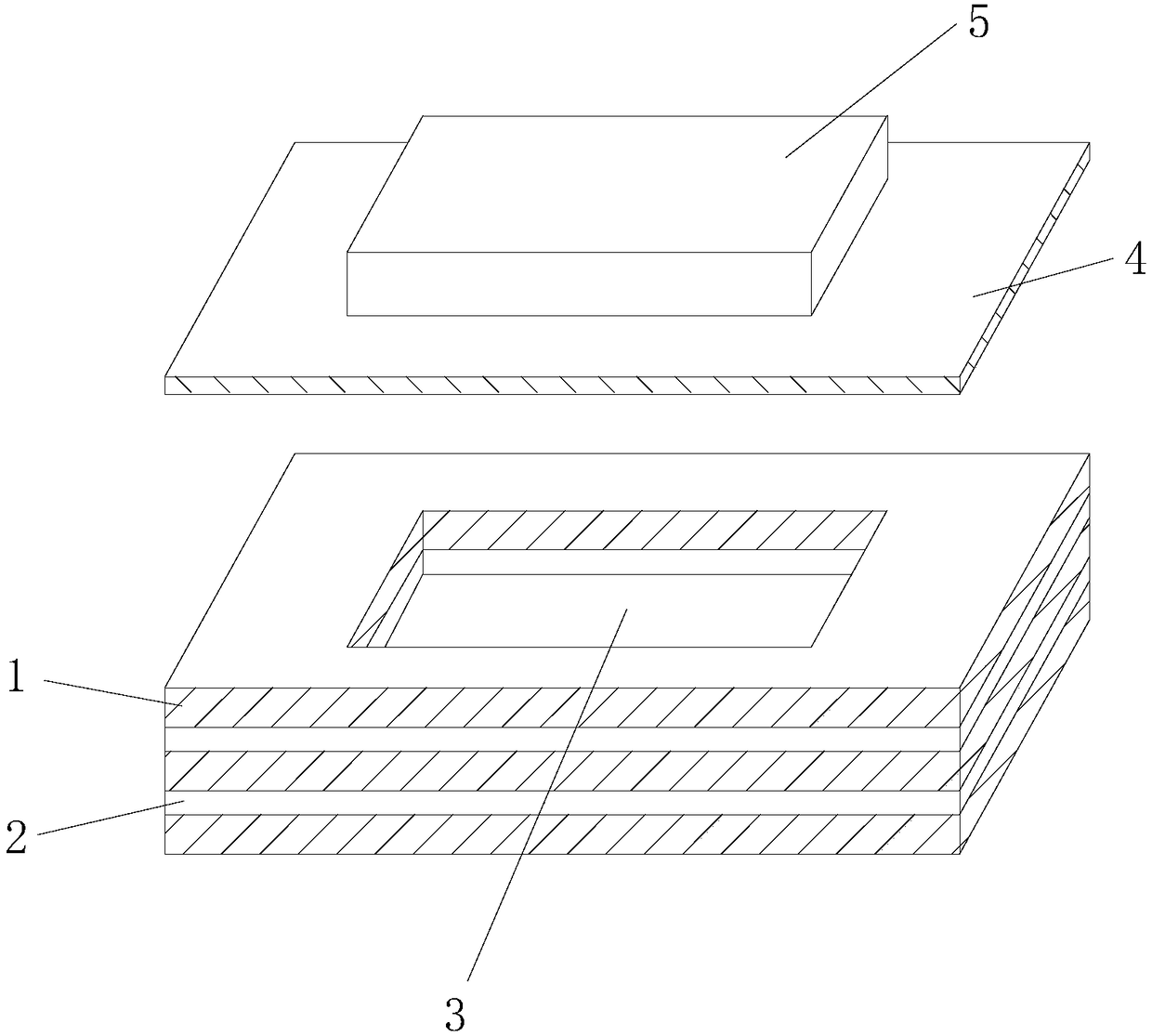
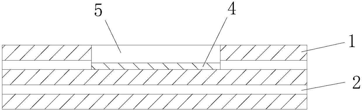
[0061] image 3It is a schematic cross-sectional view of the PCB provided in this embodiment at the position of the blind slot. Such as image 3 As shown, the groove opened on the PCB is a blind groove, and the metal block 5 and the conductive film 4 are embedded in the groove by stamping; the metal block 5 is bonded to the groove bottom of the groove through the conductive film 4 . Wherein, the size of the conductive film 4 is equal to the cross-sectional size of the groove.

[0062] Figure 4 It is a schematic cross-sectional view of the PCB provided in this embodiment at the position of the stepped blind slot. Such as Figure 4 As shown, the metal block 5 is a stepped metal block, and the groove is a stepped blind groove; the small end of the stepped metal block faces the groove bottom of the groove. The stepped plan...


PUM


Abstract

The invention discloses a PCB and a manufacturing method thereof, and relates to PCB manufacturing technologies. The manufacturing method of the PCB comprises that substrates and prepregs are provided, slots are formed in positions, into which metal blocks are embedded, of at least part of the substrates and the prepregs; all the substrates and prepregs are stacked and fixed sequentially, and grooves are formed in the positions into which metal blocks are embedded; a conducting resin sheet and a metal block are disposed above the groove; the metal block and the conducting resin sheet are stamped into the groove; and all the substrates and prepregs are laminated. A conductive and heat conducting material and the metal block can be placed in at the same time, it is not required to mill the conductive and heat conducting material into small units in advance, problems of offset, material damage and pollution due to taking the small units of the conductive and heat conducting material manually can be prevented, the production efficiency can be improved obviously, and the problem of low aligning degree can be solved.

Description

technical field [0001] The invention relates to PCB manufacturing technology, in particular to a PCB manufacturing method and the PCB. Background technique [0002] In conventional PCBs with embedded metal blocks, ordinary prepregs are used to bond the metal blocks to their adjacent circuit layers. In order to improve the electrical and thermal conductivity of this PCB, while taking into account the cost, you can choose to partially use an electrically and thermally conductive bonding material, such as a conductive film, between the metal block and the adjacent circuit layer. However, the implementation of this design is relatively complicated, and the conductive and thermally conductive bonding material needs to be cut into small units, placed between the metal block and the adjacent circuit layer, and then embedded in the metal block. The alignment between the small unit and the metal block is difficult to guarantee, and the smaller the size of the small unit of conductiv...

Claims


Application Information

Patent Timeline
Patent Type & Authority Applications(China)
IPC IPC(8): H05K3/46H05K1/02
CPCH05K3/4611H05K1/0203H05K2201/10416
Inventor 肖璐杜红兵孙梁纪成光王洪府刘梦茹
Owner DONGGUAN SHENGYI ELECTRONICS
Why Eureka
Try Eureka